Download
1 / 16
160 likes | 322 Views
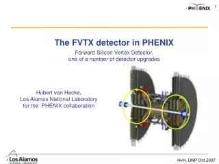
FVTX Detector Readout Concept. S. Butsyk For LANL P-25 group. Outlook. Overview of the FVTX detector LANL readout concept Read Out Card (ROC) design Front End Module (FEM) design Integration into PHENIX DAQ. FPHX Chip Data Format. Detector consists of 8640 FPHX chips

E N D
FVTX Detector Readout Concept S. Butsyk For LANL P-25 group
Outlook • Overview of the FVTX detector • LANL readout concept • Read Out Card (ROC) design • Front End Module (FEM) design • Integration into PHENIX DAQ
FPHX Chip Data Format • Detector consists of 8640 FPHX chips • FPHX chip continuously sends words with 16 bits of information at 200 MHz • Data word : contains ROW(7b), ADC(3b), BCO counter(6b) • Sync word : Sent when no data. Used to sync the serial data • 2 output lines seems to be optimal as we can output 4 hits in 4 BCO clocks • Chip designed in accordance with requirements to participate in LVL-1 trigger • Data words latch the timestamp of the beam clock in internal BCO counter • Fully programmable interface with 2 download lines per up to 32 chips
FVTX Readout Ideas • Readout is based upon PHENIX DAQ standards: • Defined set of chips is read out by a single electronics channel (FEM) through Data Collection Module (DCM) into a Packet • Granularity defined by constraints on: • Bandwidth • Readout latency (4 BCO Clocks for LVL-1) • Mechanical placement (~1.1 Mil readout channels in total, 3 times more then we currently have in PHENIX ! ) • Cost of components • R&D for the FVTX detector electronics is the same as for iFVTX detector readout • Standard DAQ implementation is a big advantage to the design • Use of well defined/tested PHENIX DAQ architecture
PHENIX Standard Part PHENIX DAQ Requirements • ~9.4 MHz beam clock • Data buffered by FEM for 64 beam clocks • LVL-1 Trigger issued with fixed delay w.r.t. collision • FEM sends the data from the collision bucket to DCM in a data packet format • Event is constructed from the packets, corresponding to the same event, by Event Builder Sub-System Dependent Part
Constraints Large number of Data I/O lines In total ~17K LVDS pairs Maximum total bandwidth 3.456 Tb/s Radiation environment around the detector 10 year Total Integrated Dose - <200 kRad 2 SEU/FPGA/hour at 40 cm for RHIC I rates Synchronicity of the data between all 8640 chips Triggered readout – data stored for less then 64 Beam Clocks Ability to generate a flag if chip clogs with data Solutions Combine/compress the data near the detector Use Radiation Tolerant FPGAs close to the detector ACTEL FLASH based FPGA Split design logically in two parts In IR – Data combiner/compressor board and fiber interface (ROC) In the Counting House – Data buffer and triggered readout (FEM) Store the data by BCO clock in 64 FIFO array Constraints for the Readout
Expected Data Rates # BCO clocks • Single wedge of FVTX detector consists of 26 FPHX chips • Simulation shows the average number of hits per chip in most central Au+Au event to be ~ 4hits/chip • Estimation of the total delay to combine and send 4 hits from every chip on 2 output lines form 52 chips takes ~14 BCO clocks • For smaller number of hits, the delay drops significantly to ~ 6 BCO clocks for 1 hit/chip 2 output lines # BCO clocks
ROC Design Specifications • Combine serial data from 52 FPHX chips • Synchronize readout and strip off Sync Words • Generate ~200 MHz Serializer Clock • Provides Control, Download and Calibration signals for the chips • Append CHIP ID to the data • Send parallel data word output at 200 MHz over 2 fiber interface to the FEM • Implemented on ACTEL A3PE3000 FLASH based FPGA
ROC Block Diagram ROC Channel FVTX Fiber Link To FEM
8-chip HDI USB Interface Actel Starter Board ROC Implementation • 4 chip combiner design implemented and tested on ACTEL test board • Ready to test the design for 8 chips combiner • Plan to test full 52 chip design by distributing the data from the single chip to 52inputs
FEM Design Specifications • FEM receives parallel data from a single ROC channel over fibers at fixed rate of 200 MHz • Main functionality • Store the data by BCO counter • Buffer data for 64 BCO clocks • Read the data from certain BCO counter to output buffer at 300 MHz • Send the output buffer content to the DCM as 20b words at 40 MHz • Plan to combine the data from 4-6 FEM channels into single DCM channel with a small-scale channel combiner FPGA • Implementation • Xilinx mid-scale Vertex-4 FPGA VC4VSX35 • Use built-in FIFOs and Relationally Placed Macros (RPMs) for maximum performance and predictability
FEM Implementation • Design tested with single chip readout and “fake” data and running chip calibration chain • 100% of hits propagates through FEM with realistic triggered readout • Readout to PC tested at 800 Mb/s rate using NI readout board Virtex-4 test board FPIX Chip
Reading from FIFO array Nothing 42 BCO clocks delay 42 BCO clocks delay Trigger Trigger Writing into FIFO array Writing into FIFO array GOT_HIT GOT_HIT Readout Prototype Testing • “Fake” LVL1 Accept generated from the FAST-OR of all pixels • Calibration board sent 100 pulses of different amplitude to a particular pixel • Design successfully run at 150 MHz input data rate
Integration into PHENIX Fiber drivers • No effect to the central arm acceptance • Total power consumption • 475 W/arm ROC board 7 ROC channels
Main Design Advantages • Reduce the number of output lines and overall bandwidth at the detector • Compatible with LVL-1 requirements • Handles Au+Au most central events with sufficient contingency • Compatible with existing PHENIX DAQ architecture • Tolerant to Single Event Upsets in radiation environment • Fits within mechanical constraints of enclosure • Reasonable power consumption • Design uses widely available and well tested commercial components