Download
1 / 35
350 likes | 506 Views
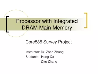
Processor with Integrated DRAM Main Memory. Cpre585 Survey Project Instructor: Dr. Zhao Zhang Students: Heng Xu Ziyu Zhang. Outline. Problem Description – CPU-DRAM Gap Latency Bandwidth Representative Papers

E N D
Processor with Integrated DRAM Main Memory Cpre585 Survey Project Instructor: Dr. Zhao Zhang Students: Heng Xu Ziyu Zhang
Outline • Problem Description – CPU-DRAM Gap • Latency • Bandwidth • Representative Papers • Missing the Memory Wall: The Case for Processor Memory Integration, ISCA 96 • A Case for Intelligent RAM: IRAM, Micro 97 • Brief Literature Review. • Conclusions and Future Research Directions
Problem Description • Processor-Memory Performance Gap • Off-chip Memory Bandwidth Limitation
Problem DescriptionProcessor-Memory Performance Gap • The development of processor and memory devices has proceeded independently. Advances in process technology, circuit design, and processor architecture have led to a near-exponential increase in processor speed and memory capacity. However, memory latencies have not improved as dramatically. • Technological trends have produced a large and growing gap between CPU and DRAM.
Von-Neumann Model • Semiconductor industry divides into microprocessor and memory camps • Separate chips, separate packages • Memory size is bigger but low power cost • CPU speed is faster and high power cost • Desktop: 1~2 CPU, 4~32 DRAMs • Server: 2~16 CPU, 32~256 DRAMs
Advantages of Von-Neumann Model • Fabrication lines can be tailored to a device • Packages are tailored to the pinout and power of a device • The number of memory chips in a computer is independent of the number of processors
Disadvantages of Von-Neumann Model • Performance gap: CPU (60% each year) vs. DRAM (7% each year) • Memory Gap Penalty: larger caches (60% on-chip area, 90% transistors) • Caches are purely performance enhancement mechanisms…. Correctness does not depend on them • No. of DRAM chips shrinking for PC config • In future it maybe a single DRAM chip • The required min. memory size, means application and OS memory use, grows only 50~75% of rate of DRAM capacity.
The Memory Latency Problem • Technological Trend: Memory latency is getting longer relative to microprocessor speed (40% per year) • Problem: Memory Latency - Conventional Memory Hierarchy Insufficient: • Many applications have large data sets that are accessed non-contiguously. • Some SPEC benchmarks spend more than half of their time stalling [Lebeck and Wood 1994]. • Domain: benchmarks with large data sets: signal processing and scientific programs
Problem DescriptionOff-chip Memory Bandwidth Limitation Pin bandwidth will be a critical consideration for future microprocessors. Many of the techniques used to tolerate growing memory latencies do so at the expense of increased bandwidth requirements. Reduction of memory latency overhead aggravates bandwidth requirement for two reasons: • First, many of the techniques that reduce latency-related stalls increase the total traffic between main memory and the processor. • Second, the reduction of memory latency overhead increases the processor bandwidth – the rate at which the processor consumes and produces operands – by reducing total execution time.
Problem DescriptionOff-chip Memory Bandwidth Limitation (Cont.) To understand where the time is spent in a complex processor, we divide execution time into three categories: • Processor time: is the time in which the processor is either fully utilized, or is only partially utilized or stalled due to lack of ILP. • Latency time: is the number of lost cycles due to untolerated, intrinsic memory latencies. • Bandwidth time: is the number of lost CPU cycles due both to contention in the memory system and to insufficient bandwidth between levels of the hierarchy.
Problem DescriptionOff-chip Memory Bandwidth Limitation (Cont.) Processor time: Latency time: Bandwidth time: Program’s execution time: Let be these times normalized to
Limitation of Present Solutions • Huge cache: • Slow and works well only if the working set fits cache and there is some kind of locality • Prefetching • Hardware prefetching • Cannot be tailored for each application • Behavior based on past and present execution-time behavior • Software prefetching • Ensure overheads of prefetching do not outweigh the benefits • Hard to insert prefetches for irregular access patterns • SMT • Enhance the utilization and throughput at thread level
Time for a Paradigm Shift…. • Missing the Memory Wall: The Case for Processor Memory Integration, ISCA 96 • A Case for Intelligent RAM: IRAM, Micro 97 • Brief Literature Review
Ground-breaking Design • Combined CPU with DRAM: merges processor and memory into a single chip. • Compare to the conventional on-chip cache: • Cache uses SRAM • Uses DRAM – since the DRAM is in practice approximately 20 times denser than SRAM
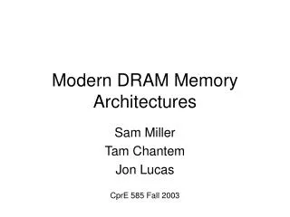
Mem Controll Serial port 4096b buf 4096b buf 512 B Victim Cache Reg File 4096b buf 4096b buf Memory Processor 16Mbit DRAM Cell 16Mbit DRAM Cell Ld/St Unit Int Unit FP Unit Branch Unit 4096b buf 4096b buf Decode Fetch An Example of Combined Design Figure: the design of combination of CPU and DRAM
Combined design features • 16 independent bank controllers are assumed in a 256Mbit device. • Each bank is capable of transferring 4K bits from the sense amplifier array to and from 3 column buffers. • Memory access time is assumed to be 30ns or 6 cycles of the 200MHz clock. • The performance of the 16KByte data cache is enhanced with a fully-associative victim cache of 16 32-Byte lines with an LRU replacement policy. • Large DRAM requires ECC protection to guard against transient bit failure. Two independent 64 (+8 for ECC) bit datapaths connect the column buffers with the processor core, one each for data and instruction access. • All off-chip communication is handled via a scalable serial link inter-connect system.
Simulation Methodology for Uniprocessor Uniprocessor performance: • The current industry-accepted-standard metric for uniprocessor performance is the SPEC95 benchmark suite. This suite of programs is supposed to represent a balanced range of uniprocessor applications, the total execution time of which is used to measure the integer and floating point performance of a processor. • As well as using this suite of applications to benchmark the proposed design, the Synopsys application was added as an example benchmark application with the large work-load of a real chip design.
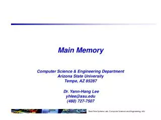
Simulation Results for Uniprocessor Figure: simulation results of data cache miss rates
Simulation Methodology for Multiprocessor Multiprocessor performance: • The simulation benchmarks are taken from the SPLASH suite. • Compared with results obtained from a reference CC-NUMA design with 16KByte direct-mapped First-Level Caches (FLCs) and infinitely sized Second-Level Caches (SLCs). • The use of infinite SLCs removes the SLC capacity misses, providing an idea upper-bound of the system performance when only the cold and the coherence misses are considered.
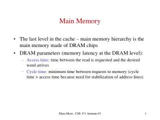
Simulation Results for Multiprocessor Figure: simulation results of multiprocessor performance
Conclusion • The trend towards larger DRAM devices exacerbates the processor / memory bottleneck, requiring costly cache hierarchies to effectively support high performance microprocessors. • A viable alternative is to move the processor closer to the memory, by integrating it onto the DRAM chip. • Processor / memory integration is advantageous, even if it requires the use of a simpler processor.
Time for a Paradigm Shift…. • Missing the Memory Wall: The Case for Processor Memory Integration, ISCA 96 • A Case for Intelligent RAM: IRAM, Micro 97 • Brief Literature Review
Intelligent RAM • Unifying processing and memory into a single chip • Using DRAM rather than SRAM • DRAM is 25~50 times denser (3D structure) • Thus on chip memory much larger • Reason of IRAM: • Memory speed limits application • Processor uses 1/3 of the die, rest place big enough for Gbit DRAM to hold whole programs • More metal layers and faster transistors in DRAM in today’s technology, make DRAM as fast and dense as conventional logic process
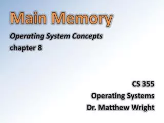
IRAM: A Chip that remembers and computes CPU CPU $ $ L2 $ DRAM DRAM Von-Neumann Model IRAM Model
IRAM potential advantage (1) • Higher bandwidth • Gbit DRAM, 3~4 metal layers • Won’t limit performance by bandwidth • Lower latency (<30ns ~ L2) • Wire length the shorter the better • Fewer bits per block the better • More design choices frees designer • Two type of application will be benefit • Predictable memory accesses: (matrix) • 50-100-fold increase in IRAM bandwidth • Unpredictable memory accesses, large footprints: (database) • 5-10 fold decrease in IRAM latency
IRAM potential advantage (2) • Better energy efficiency • Fewer external memory accesses • Save from off-chip buses • DRAM consumes less that SRAM • Flexible memory size and width • Give designer more choice, flexible than power of 2 • Save board space • Give possible to use on small handhelds
Potential disadvantages • Area and power impact of increasing bandwidth to the DRAM core • Need to add more I/O lines • More cost per bit • Retention time of DRAM core operating at high temperatures • Scaling a system beyond a single IRAM • Expandable memory • DRAM industry? • A $37 billion industry need a reform? Testing DRAM cost higher • Chip • Speed, area, power, yield in DRAM process? • Good performance and reasonable power? • BW/Latency oriented DRAM tradeoffs? • Testing Time of IRAM vs DRAM vs µP? • Architecture and Compiler • How to turn high memory bandwidth into performance for real applications?
Evaluate IRAM • From current to IRAM oriented • Alpha 21164 • An IRAM vector processor • Evaluate based on performance factors and estimates. (table 2 and table 4)
Evaluate IRAM: Alpha 21164 • Logic slow down 1.3~2.0, • SRAM to DRAM: 1.3 times slower • IRAM the time to main memory is 5~10 times faster • With complex cache hierarchy, better performance in database and matrix.
IRAM’s Energy efficiency • Expressed either Joules per instructions or MIPS per Watt better measures the energy efficiency • IRAM has advantage roughly a factor of 2 ~4.
IRAM--Summary • IRAM: Merging a microprocessor and DRAM on the same chip • Performance: • reduce latency by 5~10 • Increase bandwidth by 50~100 • Energy efficiency • Save at 2~4 • Cost • Remove off-chip memory and reduce board area • IRAM is limited by amount of memory on Chip • Potential of network computer • Change the nature of semiconductor industry
Time for a Paradigm Shift…. • Missing the Memory Wall: The Case for Processor Memory Integration, ISCA 96 • A Case for Intelligent RAM: IRAM, Micro 97 • Brief Literature Review
Brief Literature Review • Technology-level • O. Kimura, et. al. Panel Session: DRAM + Logic Integration: Which Architecture and Fabrication Process. ISSCC, 97. • System-level & Arch-level vs. Tech Level • D. Burger. System-level Implications of Processor-Memory Integration, ISCA, 97. • V. Cuppu & B. Jacob. Concurrency, Latency or System Overhead: Which has the Largest Impact on Uniprocessor DRAM-System Performance? ISCA 01. • B. Jacob. A Case for Studying DRAM Issues at the System Level. Micro, 03. • Memory-Controller based • J. Carter, et. al. Impulse: Building a Smarter Memory Controller. HPCA, 99. • Cached DRAM based • Z. Zhang, et. al. Cached DRAM for ILP Processor Memory Access Latency Reduction. Micro, 01. • New Architectural Designs • D. Burger et.al. Datascalar Architecture, ISCA, 97. • S. Swanson et al. Wavescalar. Micro, 03.
Conclusions and Future Research • Bridging the gap between CPU & DRAM is critical • More efforts should be put forth in the direction of System-level and Arch-level research
Thank you! • Any Question?