Download
1 / 18
180 likes | 312 Views
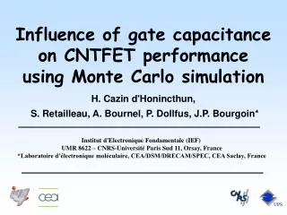
UPS. Influence of gate capacitance on CNTFET performance using Monte Carlo simulation. H. Cazin d'Honincthun, S. Retailleau, A. Bournel, P. Dollfus, J.P. Bourgoin*. Institut d'Electronique Fondamentale (IEF) UMR 8622 – CNRS-Université Paris Sud 11, Orsay, France

E N D
UPS Influence of gate capacitance on CNTFET performance using Monte Carlo simulation H. Cazin d'Honincthun, S. Retailleau, A. Bournel, P. Dollfus, J.P. Bourgoin* Institut d'Electronique Fondamentale (IEF) UMR 8622 – CNRS-Université Paris Sud 11, Orsay, France *Laboratoire d’électronique moléculaire, CEA/DSM/DRECAM/SPEC, CEA Saclay, France
Plan • Carbon nanotubes: high potential material • Carbon nanotubes: Model for calculations (Monte Carlo) • Evaluation of Mean Free Path • Carbon nanotube field effect transistor simulation
Potentialities of Carbon nanotubes • Charge transport and confinement • Charge transport is quasi-ballistic: few interactions • Charge confinement (1D): good control of electrostatics • No dangling bonds • Possibility to use High K material for oxide • Band structure « quasi » symmetric • Transport properties identical for electron and hole (same m*) • Carbon nanotubes can be either metallic as well as semi-conducting • All-nanotube-based electronic is possible
Plan • Carbon nanotubes: high potential material • Carbon nanotubes: Model for calculations (Monte Carlo) • Evaluation of Mean Free Path • Carbon nanotube field effect transistor simulation
electron - time of free flights tf - type of scattering i - effect ofscattering (DE, q) scattering rates Particle Monte-Carlo method Study of carrier transport in this work: solving the Boltzmann equationby the Monte Carlo method Statisticalsolution :by Monte Carlo method • assemblyof individual particles • 1 particle • N particles allowus to reconstruct Carrier trajectories: Succession of free flight and scattering events random selection of (Monte Carlo algorithm)
subbands 3 subbands 2 DE12 subbands 1 EG /2 Band structure and phonons • Energy dispersion calculated by: • Tight-binding • Zone-folding Phonon dispersion curves calculated by zone folding method Approximation • Longitudinal acoustic and optical modes • are considered as dominant like in graphene Analytical approximation of dispersion curves [Pennington, Phys. Rev. B 68, 045426 (2003)] + RBM phonon (ERBM ≈ Cst./dt) [M. Machon et al., Phys. Rev. B 71, 035416, (2005)] Ex: Tube index n=19, ERBM=19 meV Analytical approximation of the three first subbands
Scattering Events Calculation • Scattering rates : 1st order Perturbation Theory by deformation potential model with: Daco = 9 eV [L. Yang, M.P. Anantram et al. Phys. Rev. B 60, 13874 (1999) ] DRBM = 0.65eV/cm (for n = 19)[M. Machon et al., PRB 71, 035416 (2005)] Intrasubband acoustic scattering Elastic process Intersubband transition Inelastic process n = 19 intravalley scattering from subband 1 intervalley scattering from subband 1
Plan • Carbon nanotubes: high potential material • Carbon nanotubes: Model for calculations (Monte Carlo) • Evaluation of Mean Free Path • Carbon nanotube field effect transistor simulation
Potential of quasi-ballistic transport in the low-field regime Mean Free Path Simulation in steady-state regime The mean free path depends on diameter and electric field : lMFP=100-600 nm for elastic scattering lMFP=1000-20 nm for inelastic scattering Agreement with experimental works (L. field:300-500 nm H. Field: 10-100nm)
Plan • Carbon nanotubes: high potential material • Carbon nanotubes: Model for calculations (Monte Carlo) • Evaluation of Mean Free Path • Carbon nanotube field effect transistor simulation
EOT (nm) Oxide : HfO2 S D dt = 1.5 nm et = 0.18 nm L = 20 nm Lc = 100 nm ND=5.108/m The modelled transistor Coaxially gated carbon nanotube transistor with heavily-doped source drain extensions CNTFET • Characteristics: • Zigzag tube (19,0) - dt = 1.5nm – EG = 0.55eV • Cylindrically gated • Ohmics Contacts (heavily n-doped) • Intrinsic channel • High K gate insulator HfO2 ( EOT = 16, 1.4, 0.4, 0.1 nm - COX = 72, 210, 560,1060 pF/m)
Weak field in the channel quasi ballistic transport Conduction band First subband energy profile Weak field in the channel due to strong electrostatic gate control
Reminder : CG leads towards CQ for Cox >> CQ For Cox >> CQ quantum capacitance limit Capacitive effects Weak Field 1D low density of states Channel potential is fixed Determination of CG for low VDS: Evolution of Cox and CG as a function of 1/EOT ≈ CG tends towards 4pF/cm
ID-VGS Characteristics Expected result : ID increases with oxide capacitance Cox but limited enhancement for high COX values
Evaluation of Ballistic Transport Unstrained Si. DG-MOSFETvs c-CNTFET CNTFET : 70% of ballistic electrons at the drain end for Lch = 100nm Unstrained Si DG : 50% of ballistic electrons pour Lch =15 nm
ID-VDS characteristics Device parameters extracted from simulation (Ioff=0.1nA) VDD = 0.4V ION ≈ 10 – 30 µA. ION/ IOFF ≈ 5104– 5105 High values of S and gm are obtained Acceptable agreement with experiments * H. Dai, Nano Letter, vol.5, 345, (2005) : L=80nm, EOT=1.5nm
ION/IOFF ratio (VDD) Performances CNT for LC=100nm and VDD<0.4V Performances Si for LC=15nm and VDD>0.7V * H. Dai, Nano Letter, vol.5, 345, (2005) : L=80nm, EOT=1.5nm
Conclusion This Monte Carlo simulation of a CNTFET shows excellent performances: • Excellent electrostatic gate control (quantum capacitance regime) • High fraction of ballistic electrons in the transistor channel • High performances at relatively low power supply