Download
1 / 20
210 likes | 230 Views
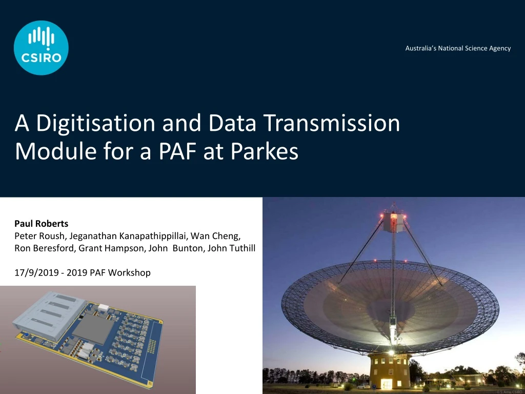
A Digitisation and Data Transmission Module for a PAF at Parkes. Paul Roberts Peter Roush, Jeganathan Kanapathippillai, Wan Cheng, Ron Beresford, Grant Hampson, John Bunton, John Tuthill 17/9/2019 - 2019 PAF Workshop. Parkes CryoPAF System Summary. System Architecture.

E N D
A Digitisation and Data Transmission Module for a PAF at Parkes Paul Roberts Peter Roush, Jeganathan Kanapathippillai, Wan Cheng, Ron Beresford, Grant Hampson, John Bunton, John Tuthill 17/9/2019 - 2019 PAF Workshop
System Architecture Warm RF Electronics Digitiser PAF Cryostat ~200m 1 GbE 100Gb Packet Data 128MHz & Time Frame Beamformer Timing Reference and Distribution Control & Monitor 10MHz 1PPS GPU Cluster Baseband RF input Direct digitisation at focus Packetised digital data transmitted Need a high integration solution=> RF to Packet Data
Xilinx RFSoC Platform – An FPGA plus more. • Four major parts to RFSOC: • Digital-RF subsystem (ADC/DAC) • Programmable logic (FPGA core fabric) • Processor System (ARM Cortex) • SerDes interfaces (high speed serial IO) • Powerful combination of four technologies in one. • High integration, performance and cost savings • Gen-1 • 16 x 2GSPS ADCs • 8 x 4GSPS ADCs
“Jimble” Board Design Philosophy 3.5cm • Simple – remote ADC/Packetiser/Transmitter applications • Small but powerful like namesake • C.f. “Bluering” for more capability • Low EMI – attention to EMI and no local CPU/DRAM etc • Reusable in other applications – 3U 100x160mm reconfigurable form factor • Data/Timing/Reference/Control interfaces – Fully optical (optional electrical) • Only electrical inputs are RF and power • Command and control 1/10 GbE
12V “Jimble” Module Hardware Overview Power Sequencing Power QSFP Signal Conditioning RF Input Xilinx RFSoC XCZU27DR QSFP 100 Gb Aurora/Enet x8 total QSFP 1GbE Signal Conditioning RF Input Buffer Amp BAT QSFP Sample Clock Synths Reference, Timing & Control VCXO Clean-up Ref 128MHz
“Jimble” Module Signal Processing Overview RF1 ADC 12bit 4.096 GS/s Packetise and Time stamp Over-sampled PDFB ~1MHz Channels 100 Gb PHY RF2 ADC 12bit 4.096 GS/s Packetise and Time stamp Over-sampled PDFB ~1MHz Channels Packet Mux and Scheduling Engine 100 Gb PHY 100 Gb PHY RF8 ADC 12bit 4.096 GS/s Packetise and Time stamp Over-sampled PDFB ~1MHz Channels
Initial Prototype results: 120 dB shielding effectiveness measured Thermal impedance ~0.35 degC/W Housed in a combined RF/Digital isolated enclosure Form factor MTP12 Ribbon – WDM & single fibres
< 100 fs RMS jitter required for 60 dB ADC SNR Design verification – Sample clock and Timing ~200m fibre <30Hz BW 128MHz REF Sample Clock Synth 4.096GHz Jitter Cleaner Loop RFSoC SFP SFP ADC CLK E/O O/E 128MHz VCXO Manchester Encoded Time Frame SFP SFP Jimble Board Optical Reference Signal Distribution over (Q)SFP 70 fs rms (300Hz-100MHz)
Design verification – signal processing Packet Engine 100GbE PHY GPU Coarse DFB 122MHz Channels Selector ADC 3.93GS/s RF IN 100GbE Monitor 4096 Ch FFB + Spectrometer ZU28 RFSoC (ZCU111) On-chip 4k Spectrum 100GbE ZCU111 GPU spectrum of a 122MHz sub-band RF IN (50-4000MHz)
Full x8 input and x8 ADC/PDFB Design at full clock rate implemented on ZCU111 Uses ~ 25% of DSP48/Logic/BRAM resources – highly efficient reuse Plenty of available headroom for control and data transmission Power = ~40 W total - measured from supply current monitors on ZCU111 Design verification – multi-channel signal processing firmware
Design verification – EMI properties of board, Power supplies, enclosures Measured EMI of intended DC/DC converters EMI emissions of ZCU111 Measured spurious contamination on ZCU111 board with spectrometer Shielding effectiveness of various enclosure concepts
Design verification – POL DC-DC Converters Measured EMC of intended DC/DC converters - Evaluated multiple DC-DC converters - Settled on LT “Silent Switcher” family Photo: Ron Beresfod Silent Switcher
Design verification – ZCU111 RFSOC board emissions • Measured while running representative design. • DC-DC Converter noise • 122 MHz Reference comb • Highlights areas that need to be mindful of in board design
Design verification EMI – ZCU111 RFSOC board High Sensitivity Integrating Spectrometer • Noise input at nominal astronomy power level • Integrated spectra 5s across 122MHz sub-bands • No evidence of spurii in any sub-bands • Differential topology and careful screening. • Confidence a spurii free design can be • achieved.
Board Geometry and Layout Quad QSFP Clock RFSoC DIN41612 DC-DC Analogue Completion of first prototype expected Nov/Dec 2019
Where does the data go => 1GHz Beamformer Repeat 3 times - one for each RFSOC QSFP Gemini FPGA LRU 4 Tera-multiply-accumulates (TMAC), 1.3 Tera-bits-per-second comms, and 24GB DDR4 memory
Summary A CryoPAFRFSoC based digitiser and data transmitter design presented Reusable in various applications Design at an advanced stage of completion All critical subsections independently breaded-boarded and tested First hardware prototype end of 2019
Thank youQuestions Astronomy and Space Science Paul Roberts+61 2 9372 4365 Paul.Roberts@csiro.au