Download
1 / 24
240 likes | 410 Views
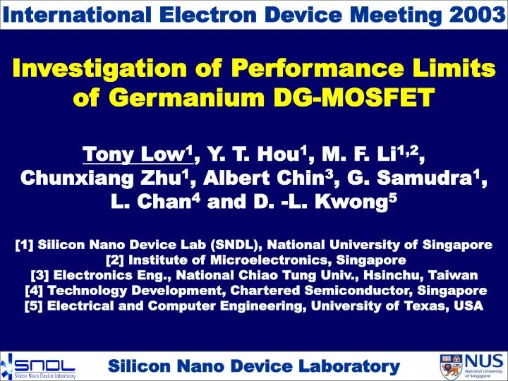
International Electron Device Meeting 2003. Investigation of Performance Limits of Germanium DG-MOSFET. Tony Low 1 , Y. T. Hou 1 , M. F. Li 1,2 , Chunxiang Zhu 1 , Albert Chin 3 , G. Samudra 1 , L. Chan 4 and D. -L. Kwong 5

E N D
International Electron Device Meeting 2003 Investigation of Performance Limits of Germanium DG-MOSFET Tony Low1, Y. T. Hou1, M. F. Li1,2, Chunxiang Zhu1, Albert Chin3, G. Samudra1, L. Chan4 and D. -L. Kwong5 [1] Silicon Nano Device Lab (SNDL), National University of Singapore [2] Institute of Microelectronics, Singapore [3] Electronics Eng., National Chiao Tung Univ., Hsinchu, Taiwan [4] Technology Development, Chartered Semiconductor, Singapore [5] Electrical and Computer Engineering, University of Texas, USA Silicon Nano Device Laboratory
Presentation Outline Motivations Modeling Methodology Impact of Surface Orientations Optimizing Ballistic Drive Current Leakage Considerations Conclusions 2
Motivations • UTB successfully demonstrated and • projected to be used in 2007 • Mobility degradations related to • body confinement and high-K dielectric S. Nakaharai et al. • High-K dielectric on Ge-Bulk or Ge-OI processing • with high mobility demonstrated • This propel recent research effort into Ge UTB Questions: • The performance limits of Ge UTB ? • The possible engineering issues ? • Prospect for future HP and LSTP applications ? 3
Quantum Simulations Straight DG MOSFET Neudeck et al. IEDM 2000 • A DG structure used, result applicable to SG at UTB • Abrupt heavily doped source/drain junctions • Lightly p-doped (1x1015cm-3) channel (NMOS) • Metal gate and EOT of 1nm used • Body thickness <5nm explored • All possible crystal orientations explored • Gate work-function selected for given IOFF • Quantum transport simulated for ION and IOFF 4
Different Surface Orientations 0.5 0.5 0.5 1 2 0.5 0.5 1 1 1 1 1 1 1 1 1 1 1 0.5 0.5 1 2 1 1 1 1 1 1 1 L valley 0.5 0.5 2 0.5 0.5 1 0.5 valley Ge<100> Ge<110> Ge<111> 2D constant energy ellipses and Brillouin zone F. Stern et al. PR163, 1967 L and valleys considered due to small energy splits Transport mass, DOS mass, Quantization mass Calculated for various surface + channel orientations L valleys electrons contribute low transport mass 5
Impact of Carrier Quantization Self-consistent Poisson and Schrodinger calculation Inversion charge: 1x1013cm-2 Body quantization effect results: L and valleys competing for dominance • valleys sink down at TBODY < 5nm for Ge<100> • L valleys dominant for Ge<110> at TBODY < 5nm • L valleys stay much below EF for Ge<111> 6
Impact of Carrier Quantization Voltage Overdrive VDD - VT VDD and VT are defined at inducing surface charge densities of 1x1013cm-2 & 1x1011cm-2 respectively • Ge UTB generally have better overdrive than Si • Ge<111> has poor overdrive due to low DOS mass 7
Ballistic Current Modeling transport current from Source to Drain NEGF Purdue’s Comp. Electronics Group • Non-Equilibrium Green Function for SD current • Scattering treated using simple Buttiker probes: A phenomenological treatment but efficient • Channel length 20nm used for good SS S. Datta et al. IEDM 2002 R. Venugopal et al. JAP 2003 8
Ballistic Current Exploring different surface and channel orientation • Ge<100> and Ge<111> relatively isotropic For Ge<110>: • Exhibits high anisotropy • Optimal channel direction for electron is [110] • Aligned with experimental optimal hole transport direction in Si <110> UTB T. Mizuno et al. VLSI 2003 9
Ballistic Current Effect of body scaling on ballistic current • Drive current decrease for Ge<100> Due to increasing valleys occupation • Drive current increase for Ge<110> Due to improved overdrive and high L occupation • Drive current decrease for Ge<111> Due to degradation of overdrive 10
Quasi-Ballistic Current TBODY=3nm LG=30nm Source/Drain mobility S. M. Sze Ge<110> 60% ballistic and Si<100> 40% ballistic Higher ballistic nature of Ge UTB due to less dissipative source/drain Ge<110> drive current at quasi-ballistic matched Si<100> ballistic current 11
Quasi-Ballistic Current Comparing performance metric CV/I of Si and Ge TBODY = 3nm LG = 30nmEOT = 1nm • Simulated at quasi-ballistic regime • Considered only subthreshold leakage • Appreciable improvement in intrinsic delay • Need to account BTB and Gate leakages in LSTP 12
Leakage Considerations for LSTP Applications
BTB Leakage Modeling of BTB Tunneling current • Subband-to-subband tunneling using WKB • Freeman and Dahlke dispersion relation used L. B. Freeman et al. SSE 1970 13
BTB Leakage BTB leakage depends on: • Effective band gap • Tunneling mass • Applied supply voltage BTB leakage sets a limit on maximum supply voltage Ge<111> exhibits very large BTB leakage 14
BTB Leakage Reduction of BTB Tunneling current Ge<110> performance diminish when BTB dominates BTB leakage has to be suppressed for LSTP Body thinning effectively increase allowable supply voltage due to apparent band gap widening 15
Gate Leakage Modeling of Gate Tunneling current CBE: Conduction electrons VBE: Valence electrons • Improved WKBtunneling model used • Wave reflection at abrupt interfaces accounted • Only dominant CBE tunneling current considered Y. T. Hou et al. IEDM 2002 16
Gate Leakage At an inversion charge of 1x1013cm-2 Gate leakage strong dependent on quantization mass Gate leakage generally larger for Ge Relatively insensitive to TBODY except Ge<110> 17
Gate Leakage Dielectric requirements for low voltage operation Gate voltage and EOT design requirements for gate leakage of 10pA/um (Inversion charge 1x1013cm-2) HfO2 with k=22 TBODY=3nm and LG=30nm Ge UTB requires a larger EOT (of ~1nm) for given gate voltage 18
Main Findings Ge UTB DG: Performance Limit & Design Requirement • Ge<110>: • Largest drive current and increase with body scaling • 2) High anisotropy of drive current • Aligned optimum channel for electron and hole transport • Require thin body for BTB suppression • Demand low voltage operation for BTB suppression • Requires larger EOT for suppression of gate leakages 19
Main Findings Ge UTB DG: Performance Limit & Design Requirement • Ge<111>: • Poor voltage overdrive • 2) Large BTB leakage • Ge<100>: • Body scaling beyond 5nm not advantageous • 2) At 5nm body, appreciable L valley electrons occupation obtainable • 3) Relatively low BTB leakages 20
Acknowledgement We acknowledge the NEGF program NanoMOS from Purdue University Comp. Electronic Group and the help rendered by Prof Mark Lundstrom, Ramesh Venugopal and useful discussion with Rahman Anisur. This work is supported by Singapore A*STAR research grant R263000267305 and R263000266305. The author T. Low gratefully acknowledges the Scholarship from Singapore Millennium Foundation. 21