Download
1 / 13
140 likes | 278 Views
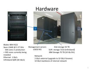
Hardware Issues. Core. Peripheral. Memory. Core. Peripheral. Memory. Peripheral. Memory. Core. Standard or system-specific bus(es). External Bus Interface. Processor Interface. Xtensa Core. Data Cache. Instruction Cache. ICache Interface. Compute Core. DCache Interface.

E N D
Core Peripheral Memory Core Peripheral Memory Peripheral Memory Core Standard or system-specific bus(es) External Bus Interface Processor Interface Xtensa Core Data Cache Instruction Cache ICache Interface Compute Core DCache Interface Instruction RAM IRAM Interface Data RAM Interface Data RAM Instruction ROM IROM Interface Data ROM Interface Data ROM XLMI Local Memories Shared Memories FIFOs Peripherals Tensilica Processor Review
Xtensa Interfaces • Instruction and data cache interfaces: • Simple synchronous SRAMs with 1(2) cycle access for data and tag arrays • Not exposed to the user by ISA simulator API • Instruction and data ROM interfaces: • Limited address range • Read only • Not useful for Smart Memories (my opinion)
Xtensa Interfaces • Instruction and data RAM interfaces • Limited address range (256 KB ?), no address translation • 1(2) cycle access • Has busy signal that must be asserted 0.5 cycles after beginning of access • Xtensa Local Memory Interface (XLMI) • Most general local data memory interface • Limited address range (256 KB), no address translation • 1(2) cycle access • Separate stall inputs for loads and stores • Supposed to be used for local or shared SRAMs, FIFOs, …
Xtensa Interfaces • Processor Interface (PIF): • Supposed to be used to access “global” memory to service cache misses • Flexible timing, i.e. hand-shake between PIF and external bus controller • Can accept inbound requests to local data RAMs
Cache coherence • Tensilica’s caches don’t support cache coherence: • Need to implement coherent caches in external hardware • But processor cache interface is just simple SRAM interface for tags and data: • Cannot do logic required for cache coherence
Solution 1 • Use instruction and data RAM interfaces to issue requests to the external memory system • Need to stall on cache miss: • Existing busy signal must be asserted 0.5 cycles after beginning of access • Better to stall processor clock: • ~1.5 cycles for cache access itself
Solution 1 • Address range limitation seems to be artificial • Not clear if instruction and data RAM address ranges can overlap • No control over store buffer: • External address translation may cause aliasing problem • Synchronization would require explicit MEMW instruction to spill store buffer
Solution 2 • Modify Tensilica’s RTL: • Need to cut out existing cache logic • Need to redefine cache interface • Not clear how hard it is • Need to do it many times • Business issues
Multiple Contexts • Currently Tensilica supports only state replication: • To switch context one has to explicitly write into control register • Tensilica plans to support switch-on-event (miss) in the future: • Switch penalty – several cycles • Not clear when it will be available
Multiple Contexts • If clock gating is used to stall processor on cache miss: • Processor can’t switch on miss • Need more flexible interface between processor and external logic: • If there is a ready context – force context switch: • Missing load must be killed • If no context is available – disable clock
Alternative Solution 1 • Use multiple cores as multiple contexts: • Easy to share caches if instruction and data RAM interfaces are used • Easily compatible with clock gating: • Only one core clock is enabled every cycle • But it’s impossible to share big expansive units: • Multiplier • FPU • SIMD unit
Alternative Solution 2 • Design our own Tensilica-compatible processor • No need for compromises: • Proper cache/memory interfaces • Can support multiple contexts • Can support special memory operations w/o high overhead • Can do address translation properly • Probably still can use some of Tensilica’s testing infrastructure • But it will require a LOT of work and cooperation with Tensilica!