Download
1 / 3
30 likes | 123 Views
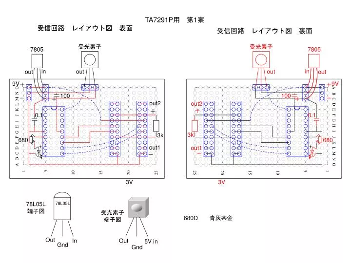
TA7291P 用 第 1 案. 受信回路 レイアウト図 表面. 受信回路 レイアウト図 裏面. 受光素子. 受光素子. 7805. 7805. in. in. out. out. out. out. 9V. 9V. +. +. 100. 100. -. -. +. +. out2. out2. +. +. 0.1. 0.1. A B C D E F G H I J K L M N O. A B C D E F G H I J K L M N O.

E N D
TA7291P用 第1案 受信回路 レイアウト図 表面 受信回路 レイアウト図 裏面 受光素子 受光素子 7805 7805 in in out out out out 9V 9V + + 100 100 - - + + out2 out2 + + 0.1 0.1 A B C D E F G H I J K L M N O A B C D E F G H I J K L M N O 3k 3k 680 680 + + out1 out1 - - 1 5 5 1 10 15 20 25 25 20 15 10 3V 3V 78L05L 端子図 78L05L 受光素子 端子図 680Ω 青灰茶金 Out In Out 5V in Gnd Gnd
TA7291P用 第2案 受信回路 レイアウト図 表面 受信回路 レイアウト図 裏面 受光素子 受光素子 7805 7805 in in out out out out 9V 9V + + 3k 3k 100 100 - - + + out2 + out1 out1 + out2 - - 0.1 0.1 A B C D E F G H I J K L M N O A B C D E F G H I J K L M N O 3V 3V 680 680 + + 1 5 5 1 10 15 20 25 25 20 15 10 78L05L 端子図 78L05L 受光素子 端子図 680Ω 青灰茶金 Out In Out 5V in Gnd Gnd
A B C D E F G H I J K L M N O A B C D E F G H I J K L M N O 1 1 5 5 10 10 15 15 20 20 25 25