Download
1 / 21
210 likes | 615 Views
MOSFET Scaling. ECE G201. next. Most Simple Model: Constant Field Scaling. E = V DD /L after scaling becomes E = (V DD / a )/(L/ a ) …where a >1. Impurity Concentration Scaling must also follow length scaling for depletion widths.

E N D
MOSFET Scaling ECE G201
next Most Simple Model: Constant Field Scaling E = VDD/L after scaling becomes E = (VDD/a)/(L/a) …where a>1
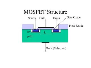
Impurity Concentration Scalingmust also follow length scaling for depletion widths Recall, that the source and drain are heavily doped and therefore the junctions are one-sided (n+p for NMOS): W = (2eVDD/qNA)1/2 …unscaled FET W/a = (2eVDD / a2qNA)1/2 = [2e(VDD/a)/qaNA]1/2 Therefore, the doping levels must increase by a factor a if the depletion widths are to scale down.
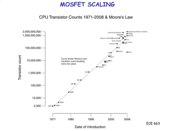
Historical Scaling“Moore’s Law:” number of transistors/chip doubles every 18 mo. 1 generation: ~18 mo. L decreases by 0.65/generation (a = 1/0.65 = 1.5) VDD decreases by 0.85/generation Therefore, constant field scaling (VDD/L) is not strictly followed.
Generalized Scaling Length: a = 1/0.65 = 1.5 Voltage: b = 1/0.85 = 1.2 Electric field:E increases x1.25 Doping: ba = x1.8 (!) note: not strictly followed
EC EV W Junction Leakage CurrentTunneling current due to highly doped Drain-Body junctions B D IJE Recall: tunneling T = Kexp(-2kW)
Gate Leakage Currenttox 0 means large tunneling current A large oxide capacitance is needed to control the channel charge and subthreshold current: Vch = VGS(Cox’+CB’)/Cox’ …where Cox’ = eox/tox since tox is limited by tunneling, research is focused on alternate gate dielectric materials with larger permittivity (“high-K”).
High-K gate insulator reduces tunneling current by allowing a thicker insulator 0.8 nm
High-K Issues • Large number of interface traps, Qit • impacts VT control and repeatability • Process integration • SiO2 is relatively easy (thermal oxidation of Si) • Potential materials: • HfO2, ZrO2, TiO2,BST….?
Scaling Directions (I)SOI (DST, depleted substrate transistor) Very thin body region (Tsi = L/3) makes the source and drain spreading resistance (RS) large. Raised S/D improves ID (next) Improves subthreshold slope, S and decreases Ioff Also decreases CjE …and IJE
Switching Speed: High current (ION) but low voltage and low IOFF
Scaling Directions (II)The “FinFET” moves from a single gate to double and triple gate structures.
Advantages: Control of the channel:must be fully depleted!Improved RS, RD due to thicker Si body
Gate prevents “top” gate Fin (30nm) BOX
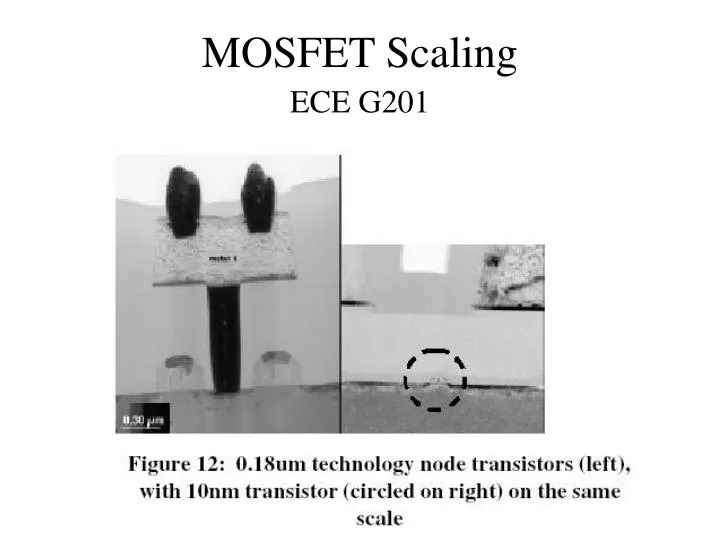
MOSFET Future (One Part of) • International Technology Roadmap for Semiconductors, 2006 update. • Look at size, manufacturing technique.
Questions? Scaling (a, e) Tunneling Subtheshold Current High-K gate dielectric Spreading Resistance (Raised S/D) FinFETs