Download
1 / 8
80 likes | 82 Views
This document outlines the status and plans for the Si/W ECal R&D project in North America, including the technologies to be tested and the goals for the test beam. It also discusses the concept, features, and ongoing R&D of the project.

E N D
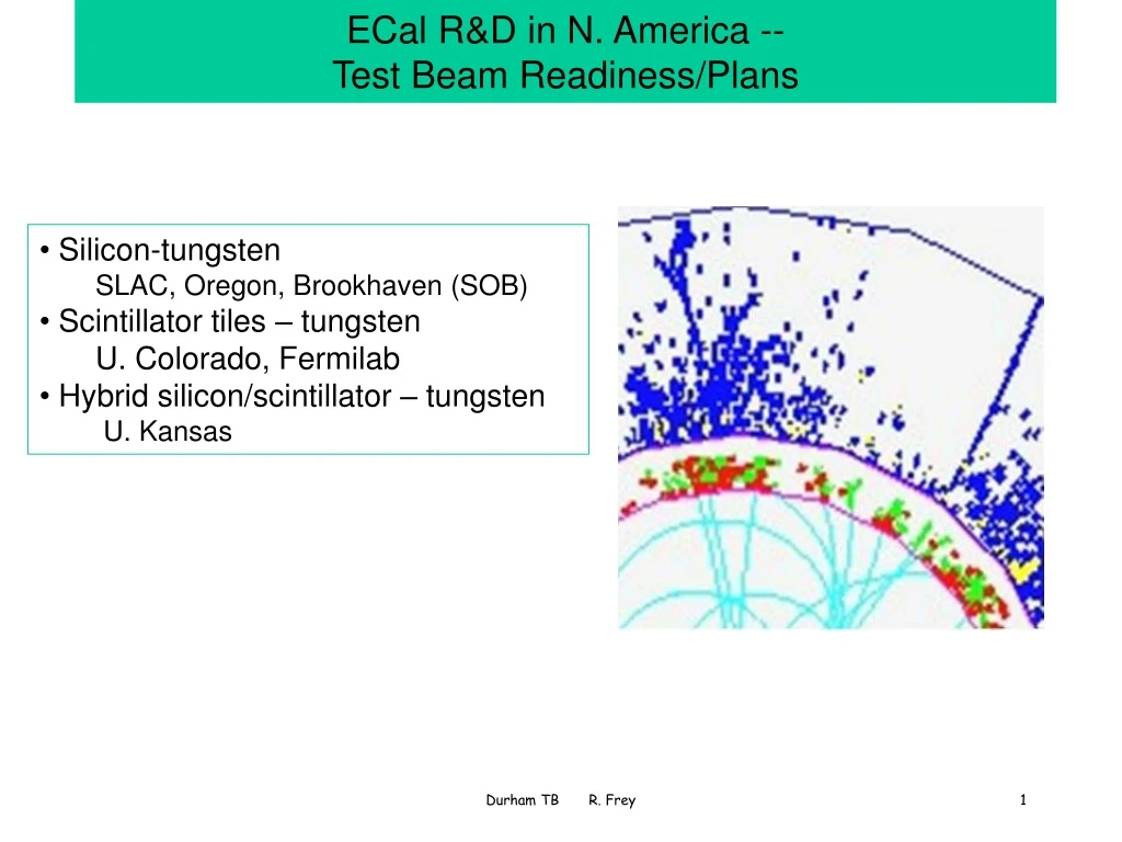
ECal R&D in N. America --Test Beam Readiness/Plans • Silicon-tungsten • SLAC, Oregon, Brookhaven (SOB) • Scintillator tiles – tungsten • U. Colorado, Fermilab • Hybrid silicon/scintillator – tungsten U. Kansas Durham TB R. Frey
Si-W Concept – SiD version 30 or fewer long. samples Durham TB R. Frey
Features • Compact (1 mm gaps) • High segmentation with little penalty • Passive cooling • Full dynamic range charge and good (few ns) timing measurements Si/W (SOB), contd • Technologies to be tested • Dynamically switched Cf • Bump bonding and on-Silicon metallizations • System-level readout resolutions
Si/W Test Beam Goals • The ECal test beam priorities are somewhat different from the HCal • A full optimization of a HCal design will likely require a hadron shower model which agrees with the test beam data. • Much of the ECal design derives from optimization of EM showers in a jet environment. • Expect – at least for front half of ECal – to be able to optimize the design independent of test beam. • First goal for test beam: Test the new technologies. • Integrated electronics and bump bonding (heat, noise, etc). • This does not require a full-depth module. • This does not require a full suite of hadron beams. • Next goal: A full-depth module. (How wide?) • Study full development of hadron showers (global Cal. priority). • Optimize back “half” ECal parameters Durham TB R. Frey
Si/W Status and Plans • Note that current design is optimized for warm, but could be optimized for cold • Would require digital pipeline → this is current focus • Would timing still be desirable? • This year • Qualify prototype detectors already in hand • Fabricate initial RO chip for technical prototype studies • Readout limited fraction of a wafer ($) (64 of 1024 chns.) • Chips probably not in hand before Jan 2005 • 2005 • Electronics evaluations • Bump bonding • “Technical” test beam, summer 2005 at earliest • A few layers with 1st round detectors and chips • Plan for a full ECal module (similar to eventual ECal) • Finalize thermal plans, mechanics • Provide correct front radiator for hadron shower validation in test beam. • Earliest beam test: Summer 2006 • Continue to evaluate configuration options • Layering, segmentation Durham TB R. Frey
Tile ECal – U. Colorado, FNAL The Basic Geometrical Structure . Durham TB R. Frey
Tile ECal (contd.) (from Uriel Nauenberg) • Will be ready for test beam in 2006 if funding becomes available in 2005 to build a module. • The big issue is electronics; we have very little help with that. • The module will consist of 60 layers or 45 layers • For 11%/root(E) resolution we need 60 layers of 1/2 X0 Tungsten and 2 mm of scintillator, not 45. • For 13%/root(E) then we can go with 45 layers of 3/4 Xo and 3 mm scintillator; (Investigating the spatial resol. deterioration.) Durham TB R. Frey
Concept: physics requires high granularity, reasonable sampling frequency, large BR2,compact RM. => ECAL probably should be W absorber, some Si, some cheaper sampling medium (Scint.). All Si is probably best IF it can be cost-effective, IF timing is not important (less so now!), and IF really large R is not dictated by the physics. All Scintillator is probably prohibitively expensive due to channel count at sufficient granularity Ongoing R&D: mostly simulation based on different design possibilities EM energy and angular response studied Photon/hadron separation in progress Critical items Does coarse scintilllator granularity work for a hybrid ? Gap size (compactness) Test-beam Wishes & Goals: could validate the EM response of hybrid ECALs with mixed sampling media Eg. Anti-correlation predicted in Si and Scint. response In collaboration with existing groups encourage that data taking opportunities with large volume HCALs and expensive Si-W ECALS can also be used to explore alternative ECAL designs to Si-W Ideally gaps eg. alveoli in the CALICE ECAL could be used to study alternative sampling layers. A hanging-file type approach would facilitate understanding the intrinsic response (but not an engineered hermetic solution …) Have funds available which can contribute significantly to a prototype ECAL construction and testing on a 2-year time-scale. Envisage wanting electron, pion beams in summer 2006 Concurrent running with HCAL activities Exactly how to proceed depends on developing collaborations and results of simulation studies (want to use test-beam time and construction funds wisely) ECAL R&D; Tungsten ECAL with both Si and Scintillator sampling Graham W. Wilson for Kansas, Kansas State Universities