Download
1 / 24
240 likes | 388 Views
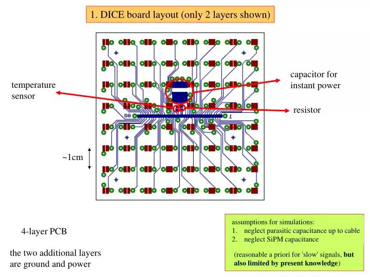
1. DICE board layout (only 2 layers shown). capacitor for instant power. temperature sensor. resistor. ~1cm. assumptions for simulations: neglect parasitic capacitance up to cable neglect SiPM capacitance. 4-layer PCB. the two additional layers are ground and power.

E N D
1. DICE board layout (only 2 layers shown) capacitor for instant power temperature sensor resistor ~1cm • assumptions for simulations: • neglect parasitic capacitance up to cable • neglect SiPM capacitance 4-layer PCB the two additional layers are ground and power (reasonable a priori for 'slow' signals, but also limited by present knowledge)
NEXT-100 SiPM plane A=8825cm2 ~8825 SiPMs (1cm pitch) ~138 Dice-Boards ~Due to fill-factor (A. Martinez): 111 Dice-Boards ~9.4mm thickness overall assuming NEXT-DEMO cable. placement of ZIF connector seems more critical. From Derek: 0.3mm x 4.5mm. 106cm 3.3cm additional thickness 25x2cm additional length possibly 2 feed-throughs are ok (will if be possible to shield the ZIF Connector from inside?)
2. DICE board schematics and cable 80 traces/cable trace pitch 0.05cm 64 signals/cable cable width = 4cm (0.05 x 80) re-done take the largest length for simulations (safe)
3. FEE take the shortest bandwidth for simulations (safe) RC=0.5-2μs (BW~600-150kHz) It seems from the datasheets of all ASICS that, if running with any recommended feedback loop, they will have a much higher bandwidth, so possibly the RC of the passive integrator dominates the response function. Better could be done if the frequency response function of the system is simulated or experimentally determined (possibly not a practical approach).
4. SiPM input signal assumed positive in the following for convenience
5. The simulation code • Based on the solutions for loss-less multi-conductor transmission lines. A convenient matrix implementation is done in Matlab/Octave (open source). Well know procedure, equivalent to pSPICE, APLAC et al. • Only losses along the conductor (resistive) or between the conductor and ground (dielectric) are considered. They are factorized from the solution. Experimentally, this seems to be a good practical approach as long as losses are not dominating the transmission (an usual desired case). • For the assessment of the present cable this has been neglected, since other effects are clearly of greater relevance.
constraints • From connector (cable geometry at the connection): • trace width = 0.3mm, pitch=0.5mm, 80 traces. Plated through hole connection. (J. Samaniego) • Connector dimensions: • thickness = 3mm, length 4.5mm. (D. Shuman, J. Samaniego) • Stiffener strip in the connection region: • 0.3mm x 4.5mm (thickness x length). (D. Shuman) • Maximum kapton thickness 127μm (in steps of 12.7μm). (J. Samaniego). • Minimum kapton thickness for a bond-ply 25 μm (D. Shuman from Fralock). • Some flexibility for easier connection inside. (D. Shuman) • Thin copper trace. Down to 5μm is possible?. (D. Shuman) • Try with Cu/Kapton/Cu/Kapton cables. (D. Shuman)
simulated NEXTDEMO cable: from MAXWELL-2D FEM solver Cm2=0.72pF/m Cm2=0.72pF/m Cm1'=1.79pF/m Cm1=20.91pF/m Cm1=20.8pF/m Cg=21.3pF/m Cm2=1.68pF/m Cm2=1.69pF/m Cg=1.19pF/m central strip boundary strip characteristic impedance (here high because the ground plane is far apart) central strip coupling coefficient (for any typical design this is usually <0.1, but here ground is far) Zc = 187 Ω Zm/Zc = 0.65 v/c = 0. 855 θ = 1.4 propagation velocity (very high since there is almost no dielectric) dispersion term (causes dispersion if much larger than one). It quantifies how much the structure differs from the propagation in a uniform media.
simulated NEXT100 cable (1): from MAXWELL-2D FEM solver Cm=0.0048 pF/m Cg=928 pF/m 500 μm 50 μm 350 μm very respectable value, almost 1nF over 1 meter 5 μm -thickness Gives 6.6mm thickness /cable characteristic impedance central strip Zc = 6.7 Ω Zm/Zc = 8e-6 v/c = 0. 5 θ = 0.0004 coupling coefficient propagation velocity dispersion term
simulated NEXT100 cable (2): from MAXWELL-2D FEM solver Cm=1.46e-9 pF/m Cg=308 pF/m 100 μm characteristic impedance central strip Zc = 19.9 Ω Zm/Zc = 2e-11 v/c = 0. 54 θ = 1.83e-9 coupling coefficient propagation velocity dispersion term
NEXTDEMO for central trace simulated cable signals
NEXTDEMO for central trace simulated cable signals
NEXTDEMO for trace close to ground (far-ground side) simulated cable signals
NEXTDEMO for trace close to ground (far-ground side) simulated cable signals
NEXTDEMO for trace close to ground (close-ground side) simulated cable signals
NEXTDEMO for trace close to ground (close-ground side) simulated cable signals
NEXT100 simulated cable signals Too low, I fear numerical problems
NEXT100 simulated cable signals full lossy
Conclusions (I) • Under present constraints, cross-talk and transmission can be improved arbitrarily by increasing the coupling to ground (certainly well below a fraction 1/250pe, where 250pe is the ADC dynamic range). Present cable design has a cross-talk of 1/10pe (different for each trace). Note: Azriel and me are thinking a bit on this, should be possible to come to a conclusion soon. He will do measurements with several capacitances in parallel at the SiPM output to see the effect. • A symmetric coupling to ground for all strips will help during later studies and data analysis. This ensures same x-talk and same noise for all traces. This is clear. • Losses (mainly resistive) seem not to be important even for 5μm (thick) x 100μm (wide) cable over 90cm. Some 10% signal decrease. Check again for 4m cable. • Cable option 1 provides a capacitancetoground of almost 1nF/m and a characteristicimpedance of 6.7 Ω. Itisessentiallythesame cable thatiscurrentlyused, butwith a groundplane and thinnercopper traces. I haveexperiencerouting HF (analog) signals in similar conditions (10Ω, 0.3nF/m), withlarger band-widthamplifiers (1.5GHz, 50Ω) and up to 1m. Noisewas tolerable fortheapplication. Converging… cable option 1 seemsthewaytogo. Ifwereplacethegroundplanebymeshesthesituationwill be much more comfortable. • A good practical condition in order not blow up the noise might be to keep the capacitance with respect to ground to the same level than the capacitance of the SiPM (?). I do not have this input. Converging… • Cable-1 keeps the pattern necessary for the ZIF connector everywhere so it opens the possibility of ordering rolls, that might save some money. This requires some discussion. I am not sure whether this is really possible. Looks impossible. However building cables of the same length and shifting them by an amount equaling the connector region (ladder instead of arrow configuration) seems possible. This might save quite some money.
Conclusions (II) • With a reducedcopperthickness, theoverall cable thicknessmight be 6.6mm/cable (thisistheabsolutemininum, since 25µm istheminimumfor a bond-plyfromFraloc and thecopperthicknesscannot be reducedbelow 5µm. Ifadditionalflexibilityisrequired, onemightconsidersegmentation. From a ‘profane’ point of view, a 2.5mm-thick cable willalwayshave a decentflexibilityexceptperhapsifitissolidcopper… (thiswould mean 3 feedthroughs). With 2 feedthroughs and theproposal in cable 1, theoverallthickness per cable willstaywithin 3mm. • Itispossibleto use meshes as ground planes. Thismightincreaseflexibility. Itisdifficulttosay, butforthepresentapplication, anymeshwith a fill-factor of 20%-50% should be ok. • As comparedto a solidgroundplane, youget: • Higher x-talktoneighbor in thesame cable. Thisis ok. • Lowercouplingtoground. Thisis ok, indeed a bit better. • Higherradiativenoise pick-up. Fine withsmallholes, duetothelargeRCs of theintegrator. Any (allowed) HF pick-up will be dumped at laterstages. • Higher inter-cable x-talk. Should be fine, needs to be studied if this solution is preferred. • From the specs of LabCircuits, that we have around, this seems clearly the way to go. • Do notforgetthatthe individual cables havefirsttogofromtheSiPMtothethick cable wheretheywill be connected. In particular weneedto decide whetherwegofor a strip-line or micro-stripdesign. Once connectedtothethick cable as long as youhave at least a groundplaneitall looks strip-line sincetheneighbor ‘closesthe box’ butitwill be different in the cable thatsticksout of theSiPM. Ifpossible I suggestto use strip-line everywheretoeasesignaltransmission and keepcharacteristicimpedance (a prejudice). The cable will be niceralso.
outlook • Repeat simulations for cable-2 up to 4 meters. Assess losses more critically. • Check inter-cable x-talk for a ground mesh. • Evaluate noise-figure. • Proceed with contacts with company.
Some extra technical questions ZIF connectors are not radio-pure (LCP might or might not), could we foresee placing them behind the copper shield?. If we lack space, perhaps 4 feedthroughs is a more rational option (then we need some 12 cm inside for the connectors, --a region that is flexible anyhow, the overall thickness per cable can be below 2mm). Connectors should be placed in a way that they will not bend towards the inner hole, so they cannot face the active region. Why not a ladder??. Then it is possible to use cables of the same length. We need some 25cm inside/feedthrough in order to stager the connectors in a ladder, do we have this space??