Download
1 / 1
10 likes | 149 Views
ADC. ADC. ADC. ADC.

E N D
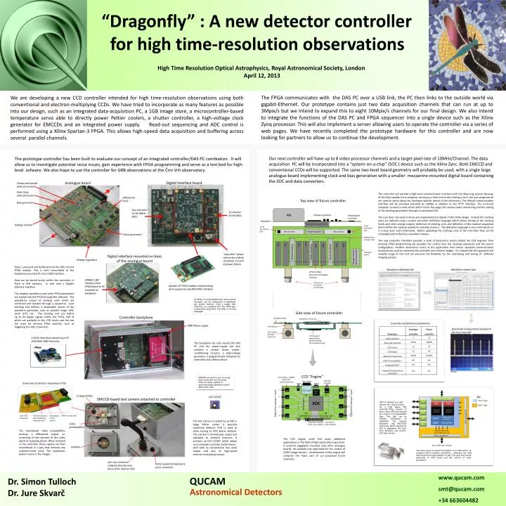
ADC ADC ADC ADC We are developing a new CCD controller intended for high time-resolution observations using both conventional and electron-multiplying CCDs. We have tried to incorporate as many features as possible into our design, such as an integrated data-acquisition PC, a 1GB image store, a microcontroller-based temperature servo able to directly power Peltier coolers, a shutter controller, a high-voltage clock generator for EMCCDs and an integrated power supply. Read-out sequencing and ADC control is performed using a Xilinx Spartan-3 FPGA. This allows high-speed data acquisition and buffering across several parallel channels. The FPGA communicates with the DAS PC over a USB link, the PC then links to the outside world via gigabit-Ethernet. Our prototype contains just two data acquisition channels that can run at up to 3Mpix/s but we intend to expand this to eight 10Mpix/s channels for our final design. We also intend to integrate the functions of the DAS PC and FPGA sequencer into a single device such as the Xilinx Zynq processor. This will also implement a server allowing users to operate the controller via a series of web pages. We have recently completed the prototype hardware for this controller and are now looking for partners to allow us to continue the development. SOC www.qucam.com smt@qucam.com +34 663604482 Dr. Simon Tulloch Dr. Jure Skvarč Astronomical Detectors “Dragonfly” : A new detector controller for high time-resolution observations Scientific CCD characterisation at Universidad Complutense LICA Laboratory High Time Resolution Optical Astrophysics, Royal Astronomical Society, London April 12, 2013 Our next controller will have up to 8 video processor channels and a target pixel rate of 10MHz/Channel. The data acquisition PC will be incorporated into a “system-on-a-chip” (SOC ) device such as the Xilinx Zync. Both EMCCD and conventional CCDs will be supported. The same two-level board geometry will probably be used, with a single large analogue board implementing clock and bias generation with a smaller mezzanine-mounted digital board containing the SOC and data converters. Theprototypecontroller has beenbuilttoevaluateour concept of anintegratedcontroller/DAS PC combiation. Itwill allowustoinvestigatepotentialnoiseissues, gainexperiencewith FPGA programming and serve as a test bedforhigh- levelsofware. Wealso hope to use thecontrollerfor GRB observations at theČrniVrhobservatory. Digital interface board Analogueboard Clamp and sample video processor CCD The controller will provide a high-level communication interface with the observing system. Because of the fully capable Linux computer serving as a front end to the clocking circuit, the user programs do not need to worry about any hardware-specific details of the electronics. The default communication interface will be provided provided by CORBA in addition to the HTTP interface. The front-end computer contains a web server which serves the pages for camera-status monitoring and the setting of the working parameters through a customised GUI. The user does not need to know any implementation details of the FPGA design. Instead the clocking units are defined using a custom controller definition language which allows setting of the clocking levels and other analog outputs, definition of clocking units and definition of the readout sequences which define the readout waveform and data readout. The definition language is very minimalistic so it is easy learn and understand. Before uploading the clocking units to the controller they can be simulated and verified by a waveform viewer. The new controller therefore provides a level of abstraction which shields the CCD engineer from learning FPGA programming yet provides full control over the clocking sequences and the sensor configuration. Another abstraction exists at the application level where standard communication protocols are used to command the controller and retrieve images. It is hoped that this approach will simplify usage of the CCD yet preserve full flexibility for the interfacing and tuning of different imaging sensors. Dual-slope video processor EMCCD HV clock Top view of future controller Biasgenerators Twochannels 16-bit 6MHz ADCs 32-channel 14-bit DACs PSU Voltage regulators Temperature controller Backplane Voltage monitor 12-bit 16 channel DAC 12-bit 16 channel DAC Bias circuitry Bias circuitry Voltage Regulator Clockgenerators Digital board on lower side Backplane VP4 VP1 VP3 VP2 VP7 VP8 VP5 VP6 Clock circuitry Clock circuitry Clock circuitry Analogue board “stay-alive” power reserve for orderly shutdown in event of power failure. Digital interface mountedon base of theanalogueboard Voltage monitor micro-controller Voltage regulators Data is acquired and bufferedfromtheADCsbythe FPGA module. This is thentransmittedtothebackplane-mounted PC via a USB2 interface. Data can bestoredlocallywithinthecontroller, in Flash or SSD memory, orsentover a Gigabit Ethernet interface. The readout waveforms and other FPGA parameters are loaded into the FPGA through the USB port. The waveforms consist of clocking units which are combined and iterated through a sequencer. Each clocking unit defines a meaningful action of the waveform generator, such as parallel image shift, serial shift, etc. The clocking unit can defineup to 64 digital signals within the FPGA, half of which are available to the CCD clocks and the rest are used for internal FPGA controls, such as triggering the ADC conversion. Waveform definition file Waveform viewer tool VP1-8=Video processor analogue circuitry 24MB/s USB interface from FPGA boardto PC mountedonbackplane Front-panel connectors to CCD head Spartan-3E FPGA module implementing clocksequencer and ADC/DAC interface An FPGA is a programable logic device whose hardware can beconfiguredtoimplementany digital function, from a simple ADC interface to a complete CPU. The FPGA logic is described using ether the VHDL or Verilog languages. Side view of future controller Controllerbackplane Analogue board Backplane connector Controller performance parameters 40W Powersupply Flex-ribbons Download configuration/waveform file into controller Front-panel Mil-style connector CCD “Engine” “CCD engine” digital board. Mounted below the analogue board 16 bit ADCs > 20MHz with 8-bit parallel interface 1.6GHz Intel Atombased Linux PC 2GB RAM, 8GB Flash disc. Ethernet interface Boot Media Thebackplanenotonlymountsthe DAS PC and thepower-supplybutalsocontains a shutter driver, power-conditioningcircuitry, a high-voltage generator, a programmabletemperaturecontroller and a Peltier driver. Power USB2 8 1 SD card ADC Clock Gen. PHY 7 2 ADC Differential analogue inputs Differential analogue inputs FPGA heatsink 6 3 ADC HV clock 5 4 2GB RAM module socketed on under-side ADC EMCCDs are abletogiveveryhigh pixel rateswithverylownoise. They are easilycapable of detecting single photons at multi-MHz pixel rates. Sequencer outputs (CCD clock outputs) Low-speed DAC interface Underside of detector head-board PCB 2-stage Peltier E2V CCD97 EMCCD-based test camera attachedtocontroller SOC or “system on a chip” devices are a logical choice for a high speed CCD controller.They conisist of one or more CPUs surrounded by a matrix of programmable logic. This logic can be flexibly configured to implement the readout sequencer and ADC/DAC interfaces whilst leaving the CPU to implement the high-level software and control-GUI web servers. CCD Peltier access hole Thermal-isolation slots bridgedby Nichromewire. Gold-plated centre section Inter-PCB connectors The test camera iscooledbyan 8W 2-stage Peltiercooler. A speciallymachined detector PCB isusedtoallowcoolingto 50oC belowambient. The camera ishermeticallysealedbutoperated at ambientpressure. Itcontainsan E2V CCD97 whichallowsustoevaluatecontroller performance with bothitsconventionallownoise output and also its high-speedelectron-multiplying output. Video preamplifiers The head-board video preamplifiers produce a differential output i.e.consisting of twoversions of the video signal of opposingphase. Whenreceived in thecontroller, thesesignals are thenrecombined in a waythatremovesanycommon-modenoise. Thissuppressespattern-noise in theimages. The CCD engine could find many additional applications in the field of high-speed data acquisition. It could be piggyback mounted onto other analogue boards, for example one optimised for the control of CMOS image sensors. Development of this engine will comprise the major part of our proposed future controller. window The Xilinx Zynq is a powerful example of an SOC device. It contains built-in memory controllers , ethernet and USB interfaces and a huge number of user I/O pins that can be dedicated to CCD clocks and the control of video processors. Jam-nut connector soldered directly onto back of the internal PCB. Peltier power/temperature servo connector. QUCAM