Download
1 / 27
270 likes | 417 Views
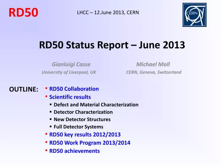
LHCC – 12.June 2013, CERN. RD50. RD50 Status Report – June 2013. Gianluigi Casse Michael Moll University of Liverpool, UK CERN , Geneva, Switzerland. OUTLINE:. RD50 Collaboration Scientific results

E N D
LHCC – 12.June 2013, CERN RD50 RD50 Status Report – June 2013 GianluigiCasse Michael MollUniversity of Liverpool, UK CERN, Geneva, Switzerland OUTLINE: • RD50 Collaboration • Scientific results • Defect and Material Characterization • Detector Characterization • New Detector Structures • Full Detector Systems • RD50 key results 2012/2013 • RD50 Work Program 2013/2014 • RD50 achievements
The RD50 Collaboration • RD50: 48 institutes and 270 members 38 European and Asian institutesBelarus (Minsk), Belgium (Louvain), Czech Republic (Prague (3x)), Finland (Helsinki, Lappeenranta ), France (Paris), Germany(Dortmund, Erfurt, Freiburg, Hamburg (2x), Karlsruhe, Munich), Italy (Bari, Florence, Padova, Perugia, Pisa, Trento), Lithuania (Vilnius), Netherlands(NIKHEF), Poland (Krakow, Warsaw(2x)), Romania (Bucharest (2x)),Russia (Moscow, St.Petersburg),Slovenia(Ljubljana), Spain (Barcelona(2x), Santander, Valencia), Switzerland (CERN, PSI), Ukraine (Kiev), United Kingdom (Glasgow, Liverpool) 7 North-American institutesCanada (Montreal), USA (BNL, Fermilab, New Mexico, Santa Cruz, Syracuse)1 Middle East instituteIsrael (Tel Aviv)1 Asian institute India (Delhi) Joined 2012/13 • Desy, Hamburg, Germany (Doris Eckstein) • IPNHE, Paris, France (Giovanni Calderini) Detailed member list: http://cern.ch/rd50 G.Casse and M.Moll, RD50 Status Report, June 2013
RD50 Organizational Structure Co-SpokespersonsGianluigi Casse and Michael Moll(Liverpool University) (CERN PH-DT) Defect / Material CharacterizationMara Bruzzi(INFN & Uni Florence) Detector CharacterizationEckhart Fretwurst(Hamburg University) Full Detector SystemsGregor Kramberger (Ljubljana University) New StructuresGiulio Pellegrini (CNM Barcelona) • LHC-like tests • Links to HEP • Links electronics R&D • Low rho strips • Sensor readout (Alibava) • Comparison: - pad-mini-full detectors - different producers • Radiation Damage in HEP detectors • Test beams (G.Casse) • Characterization ofmicroscopic propertiesof standard-, defect engineered and new materials pre- and post- irradiation • DLTS, TSC, …. • SIMS, SR, … • NIEL (calculations) • WODEAN: Workshop on Defect Analysis in Silicon Detectors(G.Lindstroem & M.Bruzzi) • Characterization of test structures (IV, CV, CCE, TCT,.) • Development and testing of defect engineered silicon devices • EPI, MCZ and other materials • NIEL (experimental) • Device modeling • Operational conditions • Common irradiations • Wafer procurement (M.Moll) • Simulations (V.Eremin) • 3D detectors • Thin detectors • Cost effective solutions • Other new structures • Detectors with internal gain (avalanche detectors) • Slim Edges • 3D (R.Bates) • Semi 3D (Z.Li) • Slim Edges (H.Sadrozinski) Collaboration Board Chair & Deputy: G.Kramberger (Ljubljana) & J.Vaitkus (Vilnius), Conference committee: U.Parzefall (Freiburg)CERN contact: M.Moll (PH-DT), Secretary: V.Wedlake (PH-DT), Budget holder & GLIMOS: M.Glaser (PH-DT) G.Casse and M.Moll, RD50 Status Report, June 2013
WODEAN project (since 2005; 10 RD50 institutes, guided by G.Lindstroem and M.Bruzzi) Aim: Identify defects responsible for Trapping, Leakage Current, Change of Neff Method: Defect Analysis on identical samples performed with the various tools available inside the RD50 network: C-DLTS(Capacitance Deep Level Transient Spectroscopy) I-DLTS (Current Deep Level Transient Spectroscopy) TSC (Thermally Stimulated Currents) PITS(Photo Induced Transient Spectroscopy) FTIR(Fourier Transform Infrared Spectroscopy) RL(Recombination Lifetime Measurements) PC(Photo Conductivity Measurements) EPR(Electron Paramagnetic Resonance) TCT(Transient Charge Technique) CV/IV >240 samples irradiated with protons, neutrons and electrons most important results published in Applied Physics Letters… significant impact of RD50 results on silicon solid state physics – defect identification Defect Characterization - WODEAN [R.Radu, 22nd RD50 Workshop, 3-5 June 2013] Example: TSC measurement on defects produced by electron irradiation (1.5 to 15 MeV) G.Casse and M.Moll, RD50 Status Report, June 2013
Microscopic Defects • Defects concentrations after electron irradiation (1.5 to 15 MeV) • Impact of oxygen content on defect formation • STFZ – Standard Floating Zone Silicon [O]=1016cm-2 • DOFZ – Diffusion Oxygenated Floating Zone Silicon [O]=1017cm-2 Defect introducing positive space charge(depending on Oxygen content) 6 MeV electrons; 1015 e/cm2; 60 min 80°C High [O] Low [O] Defect responsible for reverse annealing(not depending on Oxygen content) [R.Radu, 22nd RD50 Workshop, 3-5 June 2013; accepted for publication in NIMA] G.Casse and M.Moll, RD50 Status Report, June 2013
Microscopic Defects Results consistent with previous RD50 works on hadron damage • Some defects observed after electron irradiation (1.5 to 15 MeV) positive charge (higher introduction after proton irradiation than after neutron irradiation) leakage current+ neg. charge(current after irradiation) Reverse annealing(neg. charge) • Converging on consistent set of defects observed after proton, pion, neutron, gamma and electron irradiations by various techniques (Introduction rates depend of course strongly on the type of irradiation and for some of the defects on the material.) [R.Radu, 22nd RD50 Workshop, 3-5 June 2013] G.Casse and M.Moll, RD50 Status Report, June 2013
RD50 Simulation working group • Device simulation working group formed in 2012 (10 institutes guided by V.Eremin, Ioffe) • Aim: Produce TCAD input parameters that allow to simulate the performance of irradiated silicon sensors and eventually allow for performance predictions under various conditions (sensor material, irradiation fluence and particle, annealing). • Tools: Commercial TCAD software (Synopsis & Silvaco) and custom made software • First steps: Inter-calibration of the different tools using a predefined set of defect levels and physics parameters: All tools were able to reproduce the double-junction effect with a two level defect model. However, further tuning of defect and physics parameters is needed. Two level model: Karlsruhe University (Synopsis TCAD) Ioffe Institute (custom made software) Delhi University (Silvaco TCAD) [ RD50 Simulation Workshop – 27.3. 2013] G.Casse and M.Moll, RD50 Status Report, June 2013
RD50 Simulation working group • TCAD simulations can reproduce TCT data, leakage current, depletion voltage and (partly) charge trapping of irradiated sensors with one parameter set! • Example: Input parameter set tuned to match TCT measurements (R.Eber, Uni.Karlsruhe) • Same set of data used to simulate CCE measurements taken in a test beam (T.Peltola HIP) • Simulation predicts leakage current correctly (not shown) • Simulation predicts CCE for proton and neutron irradiated samples of different thickness within 20% • Simulations start to get predictive power; still the phase space of input parameters is huge and input (defect) parameters have to be tuned and adopted to measured defect parameters. G.Casse and M.Moll, RD50 Status Report, June 2013
Charge Multiplication • Charge Multiplication observed and characterized after high levels of irradiationwith different techniques and in several different types of devices 140 mm thick device 300 mm thick device Diodes (Feq=1016 cm-2) Leakage Current & Charge Collection Strip sensors(Feq=5×1015 cm-2, 26 MeV p) Charge Collection (Beta source, Alibava) Questions: • Can we simulate and predict charge multiplication ? • Can we better exploit charge multiplication? 3D sensors(Feq=1-2×1015 cm-2) Charge Collection (test beam) Ref: Diode: J.Lange et al, 16th RD50 Workshop, Barcelona Strip: G. Casse et al., NIMA 624, 2010, Pages 401-404 3D: M.Koehler et al., 16thRD50 Workshop, Barcelona G.Casse and M.Moll, RD50 Status Report, June 2013
Thin p-type pixel sensors • Optimizing the sensor thickness • Measurement of thin FZ p-type pixel sensors: 75, 100, 150 and 285 mm (CIS) • ATLAS FEI4; 25 MeV protons; 90Sr source • 150 mm thick devices give higher signal than 75mm and 300 mm thick devices for fluences > 1×10¹⁵neq/cm2 [Stefano Terzo (MPI), 22nd RD50 Workshop, Albuquerque, June 2013] G.Casse and M.Moll, RD50 Status Report, June 2013
Thin p-type strip sensors • Measurement of thin p-type strip sensors: 50, 100, 140 and 300 mm • MPV (mip illumination, 40MHz electronics) of sensors of various thicknesses irradiated with neutrons up to 2×10¹⁶neq cm-2. • 140 mm show good results(highest signal for > 2×10¹⁵neq/cm2) • 50 and 100 mm show stable performance over all fluence range [G.Casse, Liverpool, VCI, 2013] G.Casse and M.Moll, RD50 Status Report, June 2013
First production of low gain diodes • Diodes with implemented multiplication layer (deep p+ implant) • Following APD concept • Gain of ~10 before irradiation • Spectra are Landau spectra (90Sr) • Gain reduces with irradiation • Dropping to about 1.5 after 2e15 n/cm2.Why? Boron removal in p-type layer? • Current and noise scale as expected with multiplication • Characterization with alpha’s (Am-241) Charge/Current Multiplication (Sr-90) [G.Kramberger, 22nd RD50 Workshop, Albuquerque, June 2013] G.Casse and M.Moll, RD50 Status Report, June 2013
New structures: slim and active edges • RD50 slim edges project (reduce dead space around the active sensor) active area • Scribe present: XeF2 etch) • Cleave present: automated) • Passivateoxide (n-type) alumina ALD (p-type) slim edge inactive area guard rings [V. Fadeyev, 22nd RD50 Workshop, Albuquerque, June 2013] • Active edges (VTT & MPI Munich) • Thin wafers with active edges produced at VTT [ A.Macchiolo, 22nd RD50, Albuquerque, June 2013] 1015 p/cm2Testbeam: no difference between edge and other pixel! G.Casse and M.Moll, RD50 Status Report, June 2013
Ongoing technology studies: 3D Trench electrodes & 3D Stripixels • Exploring the possibilities of DRIE etching (BNL & CNM) • 3D sensors (well known, installed in ATLAS IBL) • 3D Trench Electrode Detectors • 3D stripixel(A single-side double strip detector) • Aim: Function as 3D but with a more homogeneous field(no saddle point) • First prototypes produced • CV/IV measured up to 100V • Next: CCE measurements G.Casse and M.Moll, RD50 Status Report, June 2013
RD50 – ALIBAVA Telescope (AT) • RD50 telescope • Alibavabased test beam telescope • Optimised for easy set-up • Fully integrated Alibavareadout • telescope and DUT have same readout • Alignment, tracking and analysis to bestandardised. Characteristics of detectors before and after irradiation, as a function of bias voltage or other variables (temperature, influence of magnetic field, etc.) can be studied in real operation conditions. • Results from DESY test beam available • Note: RD50 has access to other test beams performed in collaboration with e.g. CMS (HIP group) G.Casse and M.Moll, RD50 Status Report, June 2013
Some key results (in 2012/2013) • Progress in understanding microscopic defects • Defects responsible for positive space charge in DOFZ, MCZ and EPI and defects provoking reverse annealing are characterized! • Consistent list of defects produced covering electron, gamma, neutron and proton/pion damage • TCAD simulations : Good progress on simulations • Commercial TCAD packages well understood and proved to be well adopted to our needs (defect description) • Simulations can reproduce pulse shapes, depletion voltage, charge collection and leakage current. Getting predictive capabilities! • Systematic analysis of the Charge multiplication mechanism • Noise issue particularly important for exploitation of this feature in Experiments • New dedicated sensors produced to test avalanche effects, sensors working after irradiation • Consolidation of data obtained on p-type and thin segmented sensors • Further results on radiation tolerance and further results on long term annealing • Thin sensors seem to extend the fluence reach of silicon detectors • Slim and active edges • Further progresses towards reduction of insensitive area (edges) of detectors • New structures based on mixed technologies • Exploitation of DRIE etching: 3D-trench electrode, semi-3D sensors; planar strip with trenched electrodes, active edge planar pixel, ….….; Use of deep implantation for controlling avalanches. • Use of tools developed in framework of RD50: ALIBAVA & Edge-TCT & Beam telescope • Edge-TCT and TCT systems are now produced centrally and can be procured by interested groups • Use of the ALIBAVA readout system in many RD50 institutions; Telescope commissioned G.Casse and M.Moll, RD50 Status Report, June 2013
Workplan for 2013/2014 (1/2) • Defect and Material Characterization (Convener M.Bruzzi, INFN and University of Florence, Italy) • Consolidate list of defects and their impact on sensor properties(Input to simulation group) including introduction rates & annealing for different type of irradiations and materials • Extend work on p-type silicon • New RD50 common project: Production of test structures on p-type silicon • Review NIEL approach; Modeling and understanding role of clusters; • Detector Characterization (Convener: E.Fretwurst, University of Hamburg, Germany) • RD50 Simulation Working Group (Leader: V.Eremin, Ioffe, St.Petersburg, Russia) • Cross-calibration of different simulation tools (ongoing) • Refine defect parameters used for modeling (from effective to measured defects) • Extend modeling on charge multiplication processes • Extend experimental capacities on edge-TCT (implement set-up at more RD50 institutions) • Parameterization of electric field (fluence, annealing time, etc.) • Studies on charge multiplication processes • Continue study on “mixed” irradiations • Extend irradiation program using charged hadrons of different energy G.Casse and M.Moll, RD50 Status Report, June 2013
Workplan for 2013/2014 (2/2) • New structures (Convener: Giulio Pellegrini, CNM Barcelona, Spain) • Continue edge-TCT studies on 3D sensors • Evaluate Stripixel sensors • Characterization of dedicated avalanche test structures (devices have been produced) • Understand impact of implant shape and other geometrical parameters on avalanche processes • Combine results with edge-TCT data and simulations to get deeper understanding • Evaluate ‘low resistance strip’ sensors • Full detector systems (Convener: G.Kramberger, Ljubljana University, Slovenia) • Further studies of thin (low mass) segmented silicon devices • Study performance of thin and avalanche sensors in the time domain (Fast sensors!) • Long term annealing of segmented sensors (parameterize temperature scaling) • Continue RD50 test beam program and RD50 beam telescope • Cold irradiations and irradiations under bias (segmented detectors) • Continue study on “mixed” irradiations (segmented detectors) • Continue RD50 program on slim edges, edge passivation and active edges • Links with LHC experiments and their upgrade working groups • Continue collaboration on evaluation of radiation damage in LHC detectors • Continue common projects with LHC experiments on detector developments G.Casse and M.Moll, RD50 Status Report, June 2013
RD50 main achievements & links to LHC Experiments Some important contributions of RD50 towards the LHC upgrade detectors: • p-type silicon (brought forward by RD50 community) is now considered to be the base line option for the ATLAS Strip Tracker upgrade • n- MCZ(introduced by RD50 community) might improve performance in mixed fields due to compensation of neutron and proton damage: MCZ is under investigation in ATLAS, CMS and LHCb • Double column 3D detectors developed within RD50 with CNM and FBK. Development was picked up by ATLAS and further developed for ATLAS IBL needs. • RD50 results on very highly irradiated planar segmented sensorshave shown that these devices are afeasible option for the LHC upgrade • RD50 data are essential input parameters for planning the running scenarios for LHC experiments and their upgrades (evolution of leakage current, CCE, power consumption, noise,….). • Charge multiplicationeffect observed for heavily irradiated sensors (diodes, 3D, pixels and strips). Dedicated R&D launched in RD50 to understand underlying multiplication mechanisms, simulate them and optimize the CCE performances. Evaluating possibility to produce fast segmented sensors? • Close links to the LHC Experiments: • Many RD50 groups are involved in ATLAS, CMS and LHCb upgrade activities (natural close contact). • Common projects with Experiments: Irradiation campaigns, test beams, wafer procurement and common sensor projects. • Close collaboration with LHC Experiments on radiation damage issues of present detectors. G.Casse and M.Moll, RD50 Status Report, June 2013
Spare Slides • Some spare slides • More details on http://www.cern.ch/rd50/ • Most results presented here have been shown on the 21st or 22nd RD50 Workshop G.Casse and M.Moll, RD50 Status Report, June 2013
Microscopic Defects & NIEL • Defects concentrations after electron irradiation (1.5 to 15 MeV) • Do the defect concentrations scale with NIEL (Non Ionizing Energy Loss)? • Data taken with DOFZ – Diffusion Oxygenated Floating Zone Silicon • Defect concentrations vs. effective NIEL NIEL Damage data (leakage current) NIEL Effective NIEL • NIEL scaling (classical and effective) violated for electrons • Next step: Can we improve the NIEL scaling for hadrons by considering an effective NIEL? [R.Radu, 22nd RD50 Workshop, 3-5 June 2013] G.Casse and M.Moll, RD50 Status Report, June 2013
Edge-TCT to Study Fields [Edge-TCT, G. Kramberger, IEEE TNS, VOL. 57, NO. 4, AUGUST 2010, 2294] • Study of Electric field inside silicon sensor very challenging problem • New tool (2010): Edge-TCT (Transient Charge Technique) • Illuminate segmented sensor from the side with sub-ns infrared laser pulses • Scan across the detector thickness • Record current pulsesas function of depth • Extract rise time and collected total charge • Reconstruct the electric field • Expectations • Significant electric field only in depleted volume • Charge generated in ‘undepleted’ part of detector is lost [N.Pacifico, 20th RD50 Workshop, Bari, 2012] G.Casse and M.Moll, RD50 Status Report, June 2013
Characterizing Charge Multiplication • Long term annealing of strip sensors (HPK, 320mm thick, 75mm pitch, FZ, n-in-p) • CCE with SCT 128A (40MHz) Collected Charge from edge-TCT • Charge multiplication observed after long annealing times for high voltages • Edge-TCT • Shows CM and gives indicationfrom which depthregion charge iscollected andmultiplied [I.Mandic, 17th RD50 Workshop, CERN, Nov. 2010] [M. Milovanović, 19th RD50 Workshop, Nov.2011] G.Casse and M.Moll, RD50 Status Report, June 2013
Understanding Charge Multiplication • Exploring the effect of implant geometries • ratio of strip implant to pitch • effect of intermediate strips • effect of deeper junction • Status: Detectors produced, irradiated, measurements about to start. G.Casse and M.Moll, RD50 Status Report, June 2013
Enhancing Charge Multiplication [D.Forshaw, 19th RD50 Workshop, Nov.2011] • Strip detector Design with trenches • 5, 10, 50 mm deep trenches • 5 mm wide in center of n+ electrode Implant Poly trench 5mm trench • Sizeable effect on Charge Multiplication • Significant difference in CCE between standard and trenched detectors • Irradiation: 5×10¹⁵ neqcm-2 (neutrons) 50mm trench 10mm trench standard [G.Casse, Trento Workshop, Feb.2012] G.Casse and M.Moll, RD50 Status Report, June 2013
Thin pixel sensors • Thin pixel sensors produced: 75 and 150 mm thickness [MPI Munich] • n-in-p pixel sensors • Interconnect: Bump bonding and SLID tested [A.Macchiolo, 20th RD50 Workshop, Bari, May 2012] G.Casse and M.Moll, RD50 Status Report, June 2013
New structures: 3D sensors • 3D sensors: Mastering the technology (CNM-Barcelona, FBK-Trento) • Reproducible, reliable resultsbefore and after irradiation Double sided 3D [A.Harb (IFAE Barcelona), 19th RD50 Workshop, Nov. 2011] G.Casse and M.Moll, RD50 Status Report, June 2013