Download
1 / 34
340 likes | 449 Views
IKI10201 03b-Logic Gates. Bobby Nazief Semester-I 2005 - 2006. The materials on these slides are adopted from those in CS231’s Lecture Notes at UIUC, which is derived from Howard Huang’s work and developed by Jeff Carlyle. Road Map. Logic Gates & Flip-flops. 3. Boolean Algebra. 3. 6.

E N D
IKI1020103b-Logic Gates Bobby Nazief Semester-I 2005 - 2006 The materials on these slides are adopted from those in CS231’s Lecture Notes at UIUC, which is derived from Howard Huang’s work and developed by Jeff Carlyle.
Road Map Logic Gates &Flip-flops 3 Boolean Algebra 3 6 Finite-StateMachines 6 4 Logic DesignTechniques Sequential DesignTechniques CombinatorialComponents StorageComponents 2 Binary Systems& Data Represent. 7 5 8 Register-TransferDesign 8 Generalized FSM ProcessorComponents 9
The Modest Switch • Digital systems are basically built from an extremely simple component: • A controllable switch • The usual Electrical switch we use every day • The electric switch we use turns current on and off • But we need to turn it on and off by hand • The result of turning the switch on? • The “top end” in the figure becomes • raised to a high voltage • Which makes the current flow through the bulb • The Controllable Switch • No hands • Voltage controls if the switch is on or off • High voltage at input: switch on • Otherwise it is off
Using the switch Input Output is high (voltage) if and only if the input is high Output Now we can make one circuit control another switch… Neat! This is getting boring..
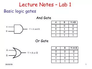
Lets use them creatively Output is high if both the inputs input1 AND input2 are high If either of the inputs is low, the output is low. Input1 Output This is called an AND gate Input2 Now, can you make an OR gate with switches?
OR Gate Input1 Output Input2 Output is low iff both inputs are low I.e. Output is high if either of the inputs (or both) are high (input1 OR input2)
How to make switches? • Use mechanical power • Use hydraulic pressure • Use electromechanical switches (electromagnet turns the switch on) • Current technology: • Semiconductor transistors • A transistor can be made to conduct electricity depending on the input on the 3rd input • CMOS “gates” (actually, switches) • We can now manufacture millions of transistors on a single silicon chip! So, switches and Gates are not magic. We know they can be built.
Basic logic gates • Each of our basic operations can be implemented in hardware using a basic logic gate. • Symbols for each of the logic gates are shown below. • These gates output the product, sum or complement of their inputs. NOT (complement) on one input AND (product) of two inputs OR (sum) of two inputs Operation: Expression: xy, or xy x + y x’ Logic gate:
Expressions and circuits • Any Boolean expression can be converted into a circuit by combining basic gates in a relatively straightforward way. • The diagram below shows the inputs and outputs of each gate. • The precedence is explicit in a circuit. Clearly, we have to make sure that the hardware does operations in the right order! (x + y’)z + x’
Exercises • Implement the following functions using 2-level gates (Sum of Product) • assume complemented literal (x’) is already available • a gate can only have 2 inputs • F1(x,y,z) = xy + yz + x’z’ • F2(x,y,z) = (x + y’)z + x’ • F3(x,y,z) = (x’ + y’)’ + xyz
Additional logic gates • NAND/NOR gates are used extensively and far more popular than AND/OR gates, simply because their implementation requires only 4 transistors (AND/OR uses 6 transistors). • NAND/NOR are faster than AND/OR NAND (NOT-AND) NOR (NOT-OR) XOR (eXclusive OR) Operation: Expressions: (xy)’ = x’ + y’ (x + y)’ = x’ y’ x y = x’y + xy’ Logic gates:
NAND gates • The NAND gate is universal: it can replace all other gates! • NOT • AND • OR (xx)’ = x’ [ because xx = x ] ((xy)’ (xy)’)’ = xy [ from NOT above ] ((xx)’ (yy)’)’ = (x’ y’)’ [ xx = x, and yy = y ] = x + y [ DeMorgan’s law ]
Making NAND circuits • The easiest way to make a NAND circuit is to start with a regular, primitive gate-based diagram. • Two-level circuits are trivial to convert, so here is a slightly more complex random example.
Converting to a NAND circuit • Step 1: Convert all AND gates to NAND gates using AND-NOT symbols, and convert all OR gates to NAND gates using NOT-OR symbols.
Converting to NAND, concluded • Step 2: Make sure you added bubbles along lines in pairs ((x’)’ = x). If not, then either add inverters or complement the input variables.
NOR gates • The NOR operation is the dual of the NAND. • NOR gates are also universal. • We can convert arbitrary circuits to NOR diagrams by following a procedure similar to the one just shown: • Step 1: Convert all OR gates to NOR gates (OR-NOT), and all AND gates to NOR gates (NOT-AND). • Step 2: Make sure that you added bubbles along lines in pairs. If not, then either add inverters or complement input variables.
XOR gates • A two-input XOR gate outputs true when exactly one of its inputs is true: • XOR corresponds more closely to typical English usage of “or,” as in “eat your vegetables or you won’t get any pudding.” • Several fascinating properties of the XOR operation: x y = x’ y + x y’
XNOR gates • Finally, the complement of the XOR function is the XNOR function. • A two-input XNOR gate is true when its inputs are equal: (x y)’ = x’y’ + xy
Extension to Multiple Inputs & Multiple Operators • Any gate can be extended to have multiple inputs as long as the binary operation it implements is commutative and associative. • AND(x,y,z,...) = (xyz...) = x y z ... • OR(x,y,z,...) = (x + y + z + ...) = x + y + z + ... • XOR(x,y,z,...) = (x y z ...) = x y z ... • XNOR(x,y,z,...) = (x y N z ...) = x y N z ... • But, • NAND(x,y,z,...) = (xyz...)’ x y z ... • NOR(x,y,z,...) = (x + y + z + ...)’ x y z ... • Multiple gates will lower the cost (smaller number of transistors) and faster circuit (smaller delay)
Logic levels • 2 voltage levels: • High (H): 5 Volts (3.3 or 1.8 Volts in some systems) • Low (L): 0 Volts • Logic gate will generate output voltage whose value represent the logical value (1 H or 0 L) • Logic gate will interpret its inputs based the input voltage (L 0 or H 1) H L
VCC(5) VCC(5.0) H H VOH(2.4) VIH(2.0) High noise margin Low noise margin VOL(0.4) VIL(0.8) L L GND(0) GND(0) Noise margins Output voltage range Input voltage range
x x’ Propagation delay • Circuits made up of gates: • If you change the inputs, and wait for a while, the correct outputs show up. • Why? Capacitive loading: • “fill up the water level” analogy. • We can use a timing diagram to show gate delays graphically. • In a circuit, when gates are connected in series, the delay will add up propagation delay gate delays
Fan-out • Using the same “fill up the water level” analogy, a single output cannot drive too many inputs: • will be too slow to “fill them up” • may not have enough power • Fan-out specifies the number of subsequent gates that can be driven by each gate, while providing voltage levels in the guaranteed range
Power dissipation • Each gate generates power dissipation during its operation; the average power dissipation is: • PTTL = Vcc (ICCH + ICCL) / 2 [for TTL] • PCMOS = Vcc ICCT [for CMOS] • PCMOS <<PTTL • Power dissipation is proportional to the heat generated by the chip • excessive heat dissipation may cause gate circuitry to drift out of its normal operating range
Gate technology • Bipolar • Transistor-transistor logic (TTL) • Emitter couple logic (ECL) • technology of the old days • MOS (metal oxide silicon) • Complementary MOS (CMOS) • low power dissipation • high fan-out • simple fabrication • higher density (number of gates per area of silicon)
Integrated Circuit (IC) technology • Small-scale integration (SSI) • 10 gates/package • Medium-scale integration (MSI) • 10 – 100 gates/package • Large-scale integration (LSI) • 100 – 1000 gates/package • Very large-scale integration (VLSI) • 1000+ gates/package (systems on a chip) • Custom design (standard cells) • Gate arrays (Gas) • Field-programmable gate arrays (FPGAs)
Full-adder design using XOR gates si = xi’yi’ci + xi’yici’ + xiyi’ci’ + xiyici = (xi’yi + xiyi’) ci’ + (xi’yi’ + xiyi)ci = (xi yi)ci’ + (xi yi)ci = (xi yi)ci’ + (xi yi)’ci = (xi yi) ci ci+1 = xi’yici + xiyi’ci + xiyici’ + xiyici = ci(xi’yi + xiyi’) + xiyi(ci’ + ci) = ci(xi yi) + xiyi longest delay = 9.0
Full-adder design using fast gates si = (xi yi)ci’ + (xi yi)ci = (xi yi)’ci’ + (xi yi)ci = (xi yi) ci xi yi = xiyi + xi’yi’ = ((xiyi)’ (xi’yi’)’)’ = ((xiyi)’ (xi + yi))’ ci+1 = xi’yici + xiyi’ci + xiyici’ + xiyici = xiyi + xici + yici = xiyi + (xi + yi)ci = ((xiyi)’ ((xi + yi)ci)’)’ longest delay = 7.6
Full-adder design using multiple-inputs gates si = xi’yi’ci + xi’yici’ + xiyi’ci’ + xiyici = ((xi’yi’ci + xi’yici’)’ (xiyi’ci’ + xiyici)’)’ = ((xi’yi’ci)’ (xi’yici’)’ (xiyi’ci’ )’ (xiyici)’)’ ci+1 = xiyi + xici + yici = ((xiyi)’ (xici )’ (yici )’)’ longest delay = 4.0