Download
1 / 18
180 likes | 366 Views
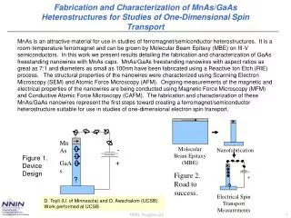
Virtual NanoFab A Silicon NanoFabrication Trainer. Nick Reeder, Sinclair Community College Andrew Sarangan , University of Dayton Jamshid Moradmand , Sinclair Community College. Challenge: Providing Hands-on Silicon Nanofabrication Experience.

E N D
Virtual NanoFabA Silicon NanoFabrication Trainer Nick Reeder, Sinclair Community College Andrew Sarangan, University of Dayton JamshidMoradmand, Sinclair Community College
Challenge: Providing Hands-on Silicon Nanofabrication Experience • The facilities needed to do silicon nanofab are very expensive.
Solution: Virtual Nanofab • Software that we’re developing to teach students about the steps involved in processing a silicon wafer. • Please take a copy of the installation disc! • System Requirements: • Operating system: Windows XP or higher • Memory: 2 GB RAM • Hard drive: 300 MB of free space • If your computer does not have National Instruments LabVIEW installed, you must install the free LabVIEW run-time engine, which is included on the installation disc.
Example: Fabricating a MOSFET • MOSFET = Metal-oxide-semiconductor field effect transistor
MOSFET in Virtual NanoFab The structure shown required about 25 steps.
User Operations • Thermal oxidation • Photolithography • Spin coat • Mask • Expose • Develop • Removing material • Wet etch • Dry etch • Depositing layers of material • E-beam evaporation • Chemical Vapor Deposition (CVD) • Sputtering • Ion implantation (“doping”)
Thermal Oxidation • Grows a layer of silicon dioxide (SiO2) on the wafer surface. • Key properties of SiO2: • Impervious to ion implantation. • Can be etched away by immersion in hydrofluoric acid (HF), which does not etch silicon.
Photolithography • Steps in photolithography: • Spin-coat photoresist. • Create and place mask. Mask defines which areas will be exposed to UV light and which areas will be shaded. • Expose with UV light. • “Develop” the photoresist: UV-exposed areas are removed, while shaded areas remain.
Photolithography in Virtual NanoFab • Before exposing: • After exposing (but before developing): • After developing:
Exposure with Uneven Layer Thicknesses Note that resist above silicon is more fully exposed than resist above aluminum.
Removing material • Methods of removing material • Wet etching • Low-tech • Immerse wafer in a bath of liquid acid or solvent • Dry etching • High-tech • Expose wafer to plasma beam
Etching in Virtual NanoFab SiO2 (blue) after wet etch with hydrofluoric acid: note tapered sidewalls and undercut of photoresist (pink). SiO2 after dry etch with CF4 plasma: note vertical sidewalls.
Depositing Layers • Methods of depositing materials • Electron-beam evaporation • Chemical vapor deposition (CVD) • Sputtering
Deposition in Virtual NanoFab Evaporated titanium (gray): accumulates only on horizontal surfaces. Chemical-vapor-deposited titanium: adheres to vertical surfaces as well as horizontal.
Ion Implantation • Modifies the electrical characteristics of the silicon wafer: key to the operation of semiconductor devices such as diodes and transistors. • Implanting boron results in “p-type” doping. • Implanting phosphorus results in “n-type” doping.
Other Features • Maintains history of user operations. • “Reference & Videos” page provides chapters explaining theory, along with videos of operations being performed in the lab.