Download
1 / 36
360 likes | 371 Views
This review discusses the levels, access times, and implementation technology of the memory hierarchy. It also explains different cache organizations and replacement policies, and analyzes cache performance with various cache sizes and associativities.

E N D
Appendix B Review of Memory Hierarchy
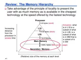
Figure B.1 The typical levels in the hierarchy slow down and get larger as we move away from the processor for a large workstation or small server. Embedded computers might have no disk storage and much smaller memories and caches. Increasingly, FLASH is replacing magnetic disks, at least for first level file storage. The access times increase as we move to lower levels of the hierarchy, which makes it feasible to manage the transfer less responsively. The implementation technology shows the typical technology used for these functions. The access time is given in nanoseconds for typical values in 2017; these times will decrease over time. Bandwidth is given in megabytes per second between levels in the memory hierarchy. Bandwidth for disk/FLASH storage includes both the media and the buffered interfaces.
Figure B.2 This example cache has eight block frames and memory has 32 blocks. The three options for caches are shown left to right. In fully associative, block 12 from the lower level can go into any of the eight block frames of the cache. With direct mapped, block 12 can only be placed into block frame 4 (12 modulo 8). Set associative, which has some of both features, allows the block to be placed anywhere in set 0 (12 modulo 4). With two blocks per set, this means block 12 can be placed either in block 0 or in block 1 of the cache. Real caches contain thousands of block frames, and real memories contain millions of blocks. The set associative organization has four sets with two blocks per set, called two-way set associative. Assume that there is nothing in the cache and that the block address in question identifies lower-level block 12.
Figure B.3 The three portions of an address in a set associative or direct-mapped cache. The tag is used to check all the blocks in the set, and the index is used to select the set. The block offset is the address of the desired data within the block. Fully associative caches have no index field.
Figure B.4 Data cache misses per 1000 instructions comparing least recently used, random, and first in, first out replacement for several sizes and associativities. There is little difference between LRU and random for the largest size cache, with LRU outperforming the others for smaller caches. FIFO generally outperforms random in the smaller cache sizes. These data were collected for a block size of 64 bytes for the Alpha architecture using 10 SPEC2000 benchmarks. Five are from SPECint2000 (gap, gcc, gzip, mcf, and perl) and five are from SPECfp2000 (applu, art, equake, lucas, and swim). We will use this computer and these benchmarks in most figures in this appendix.
Figure B.5 The organization of the data cache in the Opteron microprocessor. The 64 KiB cache is two-way set associative with 64-byte blocks. The 9-bit index selects among 512 sets. The four steps of a read hit, shown as circled numbers in order of occurrence, label this organization. Three bits of the block offset join the index to supply the RAM address to select the proper 8 bytes. Thus, the cache holds two groups of 4096 64-bit words, with each group containing half of the 512 sets. Although not exercised in this example, the line from lower-level memory to the cache is used on a miss to load the cache. The size of address leaving the processor is 40 bits because it is a physical address and not a virtual address. Figure B.24 on page B-47 explains how the Opteron maps from virtual to physical for a cache access.
Figure B.6 Miss per 1000 instructions for instruction, data, and unified caches of different sizes. The percentage of instruction references is about 74%. The data are for two-way associative caches with 64-byte blocks for the same computer and benchmarks as Figure B.4.
Figure B.7 Summary of performance equations in this appendix. The first equation calculates the cache index size, and the rest help evaluate performance. The final two equations deal with multilevel caches, which are explained early in the next section. They are included here to help make the figure a useful reference.
Figure B.8 Total miss rate for each size cache and percentage of each according to the three C's. Compulsory misses are independent of cache size, while capacity misses decrease as capacity increases, and conflict misses decrease as associativity increases. Figure B.9 shows the same information graphically. Note that a direct-mapped cache of size N has about the same miss rate as a two-way set-associative cache of size N/2 up through 128 K. Caches larger than 128 KiB do not prove that rule. Note that the Capacity column is also the fully associative miss rate. Data were collected as in Figure B.4 using LRU replacement.
Figure B.9 Total miss rate (top) and distribution of miss rate (bottom) for each size cache according to the three C's for the data in Figure B.8. The top diagram shows the actual data cache miss rates, while the bottom diagram shows the percentage in each category. (Space allows the graphs to show one extra cache size than can fit in Figure B.8.)
Figure B.10 Miss rate versus block size for five different-sized caches. Note that miss rate actually goes up if the block size is too large relative to the cache size. Each line represents a cache of different size. Figure B.11 shows the data used to plot these lines. Unfortunately, SPEC2000 traces would take too long if block size were included, so these data are based on SPEC92 on a DECstation 5000 (Gee et al. 1993).
Figure B.11 Actual miss rate versus block size for the five different-sized caches in Figure B.10. Note that for a 4 KiB cache, 256-byte blocks have a higher miss rate than 32-byte blocks. In this example, the cache would have to be 256 KiB in order for a 256-byte block to decrease misses.
Figure B.12 Average memory access time versus block size for five different-sized caches in Figure B.10. Block sizes of 32 and 64 bytes dominate. The smallest average time per cache size is boldfaced.
Figure B.13 Average memory access time using miss rates in Figure B.8 for parameters in the example.Boldface type means that this time is higher than the number to the left, that is, higher associativity increases average memory access time.
Figure B.14 Miss rates versus cache size for multilevel caches. Second-level caches smaller than the sum of the two 64 KiB first-level caches make little sense, as reflected in the high miss rates. After 256 KiB the single cache is within 10% of the global miss rates. The miss rate of a single-level cache versus size is plotted against the local miss rate and global miss rate of a second-level cache using a 32 KiB first-level cache. The L2 caches (unified) were two-way set associative with replacement. Each had split L1 instruction and data caches that were 64 KiB two-way set associative with LRU replacement. The block size for both L1 and L2 caches was 64 bytes. Data were collected as in Figure B.4.
Figure B.15 Relative execution time by second-level cache size. The two bars are for different clock cycles for an L2 cache hit. The reference execution time of 1.00 is for an 8192 KiB second-level cache with a 1-clock-cycle latency on a second-level hit. These data were collected the same way as in Figure B.14, using a simulator to imitate the Alpha 21264.
Figure B.16 Miss rate versus virtually addressed cache size of a program measured three ways: without process switches (uniprocess), with process switches using a process-identifier tag (PID), and with process switches but without PIDs (purge). PIDs increase the uniprocess absolute miss rate by 0.3%–0.6% and save 0.6%–4.3% over purging. Agarwal (1987) collected these statistics for the Ultrix operating system running on a VAX, assuming direct-mapped caches with a block size of 16 bytes. Note that the miss rate goes up from 128 to 256 K. Such nonintuitive behavior can occur in caches because changing size changes the mapping of memory blocks onto cache blocks, which can change the conflict miss rate.
Figure B.17 The overall picture of a hypothetical memory hierarchy going from virtual address to L2 cache access. The page size is 16 KiB. The TLB is two-way set associative with 256 entries. The L1 cache is a direct-mapped 16 KiB, and the L2 cache is a four-way set associative with a total of 4 MiB. Both use 64-byte blocks. The virtual address is 64 bits and the physical address is 40 bits.
Figure B.18 Summary of basic cache optimizations showing impact on cache performance and complexity for the techniques in this appendix. Generally a technique helps only one factor. + means that the technique improves the factor, – means it hurts that factor, and blank means it has no impact. The complexity measure is subjective, with 0 being the easiest and 3 being a challenge.
Figure B.19 The logical program in its contiguous virtual address space is shown on the left. It consists of four pages, A, B, C, and D. The actual location of three of the blocks is in physical main memory and the other is located on the disk.
Figure B.20 Typical ranges of parameters for caches and virtual memory. Virtual memory parameters represent increases of 10–1,000,000 times over cache parameters. Usually, first-level caches contain at most 1 MiB of data, whereas physical memory contains 256 MiB to 1 TB.
Figure B.21 Example of how paging and segmentation divide a program.
Figure B.22 Paging versus segmentation. Both can waste memory, depending on the block size and how well the segments fit together in main memory. Programming languages with unrestricted pointers require both the segment and the address to be passed. A hybrid approach, called paged segments, shoots for the best of both worlds: segments are composed of pages, so replacing a block is easy, yet a segment may be treated as a logical unit.
Figure B.23 The mapping of a virtual address to a physical address via a page table.
Figure B.24 Operation of the Opteron data TLB during address translation. The four steps of a TLB hit are shown as circled numbers. This TLB has 40 entries. Section B.5 describes the various protection and access fields of an Opteron page table entry.
Figure B.25 The overall picture of a hypothetical memory hierarchy going from virtual address to L2 cache access. The page size is 8 KiB. The TLB is direct mapped with 256 entries. The L1 cache is a direct-mapped 8 KiB, and the L2 cache is a direct-mapped 4 MiB. Both use 64-byte blocks. The virtual address is 64 bits and the physical address is 41 bits. The primary difference between this simple figure and a real cache is replication of pieces of this figure.
Figure B.26 The IA-32 segment descriptors are distinguished by bits in the attributes field. Base, limit, present, readable, and writable are all self-explanatory. D gives the default addressing size of the instructions: 16 bits or 32 bits. G gives the granularity of the segment limit: 0 means in bytes and 1 means in 4 KiB pages. G is set to 1 when paging is turned on to set the size of the page tables. DPL means descriptor privilege level—this is checked against the code privilege level to see if the access will be allowed. Conforming says the code takes on the privilege level of the code being called rather than the privilege level of the caller; it is used for library routines. The expand-down field flips the check to let the base field be the high-water mark and the limit field be the low-water mark. As you might expect, this is used for stack segments that grow down. Word count controls the number of words copied from the current stack to the new stack on a call gate. The other two fields of the call gate descriptor, destination selector and destination offset, select the descriptor of the destination of the call and the offset into it, respectively. There are many more than these three segment descriptors in the IA-32 protection model.
Figure B.27 The mapping of an Opteron virtual address. The Opteron virtual memory implementation with four page table levels supports an effective physical address size of 40 bits. Each page table has 512 entries, so each level field is 9 bits wide. The AMD64 architecture document allows the virtual address size to grow from the current 48 bits to 64 bits, and the physical address size to grow from the current 40 bits to 52 bits.
Figure B.28 Memory hierarchy parameters of the Opteron L1 and L2 instruction and data TLBs.
Figure B.29 Misses and time spent in misses for applications and operating system. The operating system adds about 25% to the execution time of the application. Each processor has a 64 KiB instruction cache and a two-level data cache with 64 KiB in the first level and 256 KiB in the second level; all caches are direct mapped with 16-byte blocks. Collected on Silicon Graphics POWER station 4D/340, a multiprocessor with four 33 MHz R3000 processors running three application workloads under a UNIX System V—Pmake, a parallel compile of 56 files; Multipgm, the parallel numeric program MP3D running concurrently with Pmake and a five-screen edit session; and Oracle, running a restricted version of the TP-1 benchmark using the Oracle database. Data from Torrellas, J., Gupta, A., Hennessy, J., 1992. Characterizing the caching and synchronization performance of a multiprocessor operating system. In: Proceedings of the Fifth International Conference on Architectural Support for Programming Languages and Operating Systems (ASPLOS), October 12–15, 1992, Boston (SIGPLAN Notices 27:9 (September)), pp. 162–174.
Figure B.30 Memory blocks distributed to direct-mapped cache.
Figure B.31 Power consumption costs of different operations.