Download
1 / 40
610 likes | 1.16k Views
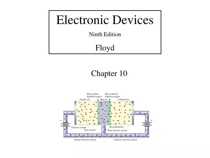
Electronic Devices Ninth Edition Floyd. Chapter 10. Summary. Effect of Coupling Capacitors. Coupling capacitors are in series with the signal and are part of a high-pass filter network. They affect the low-frequency response of the amplifier.

E N D
Electronic Devices Ninth Edition Floyd Chapter 10
Summary Effect of Coupling Capacitors Coupling capacitors are in series with the signal and are part of a high-pass filter network. They affect the low-frequency response of the amplifier. The equivalent circuit for C1 is a high-pass filter: C3 and (RC + RL) form another high-pass filter.
Summary Effect of Coupling Capacitors With FETs, the input coupling capacitor is almost always smaller because of the high input resistance. The output capacitor may be smaller or larger depending on the drain and load resistor size. For the circuit shown, the equivalent low-pass filter for the input is simply C1 in series with RG because the gate input resistance is so high.
Summary Effect of Bypass Capacitors A bypass capacitor causes reduced gain at low-frequencies and has a high-pass filter response. The resistors “seen” by the bypass capacitor include RE, re’, and the bias resistors. The equivalent high-pass filter for C2 is: Question: How would an emitter swamping resistor affect the response? fc would be lower due to increased R.
Summary Internal Capacitances The high-frequency response of an amplifier is determined by internal junction capacitances. These capacitances form low-pass filters with the external resistors. Sometimes a designer will add an external parallel capacitor to deliberately reduce the high frequency response.
Summary Miller’s Theorem Miller’s theorem states that, for inverting amplifiers, the capacitance between the input and output is equivalent to separate input and output capacitances to ground. Av is the absolute value of the gain. For the input capacitance, the gain has a large effect on the equivalent capacitance, which is an important consideration when using inverting amplifiers.
Summary Miller’s Theorem Notice that the effect of Miller’s theorem is an equivalent capacitance to ground, which shunts high frequencies to ground and reduces the gain as frequency is increased. Example: What is the input capacitance for a 2N3904 inverting amplifier with a gain of 25? Assume the values of Cbc = 4 pF and Cbe = 6 pF. Solution: Cin = Cbc(Av + 1) + Cbe Cin = 4 pF(25 + 1) + 6 pF = 110 pF
Summary The Decibel The decibel is a logarithmic ratio of two power levels and is used in electronics work in gain or attenuation measurements. Decibels can be expressed as a voltage ratio when the voltages are measured in the same impedance. To express power gain in decibels, the formula is Ap(dB) = 10 log Ap To express voltage gain in decibels, the formula is Av(dB) = 20 log Av
Summary The Decibel Sometimes, 0 dB is assigned as a convenient reference level for comparison. Then, other power or voltage levels are shown with respect to 0 dB. Some useful decibel ratios to remember are: The -3 dB power gain corresponds to a power reduction of one-half. The frequency at which this occurs is referred to as the critical frequency.
Summary Low-Frequency Response In capacitively coupled amplifiers, the coupling and bypass capacitors affect the low frequency cutoff. These capacitors form a high-pass filter with circuit resistances. A typical BJT amplifier has three high-pass filters. For example, the input coupling capacitor forms a high-pass filter with the input resistance of the amplifier:
Summary Low-Frequency Response The output RC circuit is composed of the series combination of the collector and load resistors with the output capacitor. The cutoff frequency due to the output circuit is
Summary Low-Frequency Response Example: What is the lower cutoff frequency due to C1? Assume re’ = 3.5 W and b = 200. Solution: RE1 is not bypassed, so it is added to re’. Then: = 2.77 kW 57 Hz
Summary Low-Frequency Response The bypass RC circuit response can be found by observing the charge/discharge paths. For this circuit, there is one path through RE2. A second path goes through RE1, re’, and the parallel combination of bias and source resistances (source resistance not shown). The total resistance of the paths can be found by:
Summary Low-Frequency Response Example: What is the critical frequency due to the bypass RC circuit? (Assume Rs = 600 W and b = 200 and re’ = 2.6 W). Solution: = 79.7 W 42.5 Hz
Summary Low-Frequency Response The input RC circuit for a FET is a basic high-pass filter consisting of the bias resistor (or resistors) and the input coupling capacitor. The FET gate circuit has such high resistance, it can be ignored. Example: What is the critical frequency due to the input RC circuit? Solution: 1.6 Hz
Summary The Bode Plot The Bode plot is a plot of decibel voltage gain verses frequency. The frequency axis is logarithmic; the decibel gain is plotted on a linear scale. The -3dB point is the critical frequency.
Connect the IN of the plotter on a constant level to the left of the Thevenin source. Set the cursor 3dB below the midband gain and read fc. Summary The Bode Plot Multisim has a fictitious instrument called the Bode plotter. This is the previous BJT amplifier. The Bode plotter allows you to see the Bode plot directly. By selecting the proper scales, you can magnify the response. Move the cursor to the point where the total response is – 3dB from midband and read fc.
Summary High-Frequency Response The high frequency response of inverting amplifiers is primarily determined by the transistor’s internal capacitance and the Miller effect. The equivalent high-frequency ac circuit is shown for a voltage-divider biased CE amplifier with a fully bypassed emitter resistor.
Summary High-Frequency Response If there is an unbypassed emitter resistor, such as RE1 in the earlier example, it is shown in the emitter circuit and acts to increase re’ and thus reduce fc.
Summary High-Frequency Response For the fully bypassed case, such as the one shown in the text in Example 10-11, the ac emitter resistance (re’) is multiplied by bac to obtain the equivalent input resistance at the transistor’s base.
Summary High-Frequency Response Combining the capacitors in parallel and Thevenizing forms an equivalent basic RC low-pass filter:
Summary High-Frequency Response If there is an unbypassed emitter resistor (RE1 in this case), the Thevenin resistance is modified to
Summary High-Frequency Response Example: What is the upper cutoff frequency due to the input circuit? Assume RS = 600 W, re’ = 3.5 W, b = 200, Cbe= 6 pF, Cbc = 3.5 pF, and Av = 9.7 Solution: 7.4 MHz
Summary High-Frequency Response The high frequency analysis of FETs is similar to that of BJTs. Like the CE amplifier, the CS amplifier inverts the signal, so the Miller effect must be taken into account. You may see special circuits such as cascode connections in very high frequency applications to minimize the Miller effect. A high frequency ac model of a CS amplifier is:
Summary Total Amplifier-Frequency Response In general, the overall frequency response is the combination of three lower critical frequencies due to coupling and bypass capacitors and two upper critical frequencies due to internal capacitances. The ideal Bode plot for a typical amplifier is: The bandwidth is measured between the dominant critical frequencies. BW
Summary Total Amplifier-Frequency Response The overall response can be viewed on the Bode plotter by choosing the appropriate scales. The overall response for the BJT example given previously is shown.
Summary Total Amplifier-Frequency Response For multistage amplifiers, the individual stages have an effect on the overall response. In general, with different cutoff frequencies, the dominant lower cutoff frequency is equal to the highestfcl; the dominant upper critical frequency is equal to lowestfcu. When the critical frequencies for multistage amplifiers are equal, the lower critical frequency is higher than any one as given by and the upper critical frequency is given by
Key Terms A logarithmic measure of the ratio of one power level to another or one voltage to another. Decibel Midrange gain Critical frequency The gain that occurs for the range of frequencies between the lower and upper critical frequencies. The frequency at which the response of an amplifier or filter is 3 dB less than at midrange
Key Terms Roll-off Decade Bode Plot Bandwidth The rate of decrease in the gain of an amplifier above or below the critical frequencies. A tem times increase or decrease in the value of a quantity such as frequency. An idealized graph of the gain in dB verses frequency used to graphically illustrate the response of an amplifier or filter. The characteristic of certain types of electronic circuits that specifies the usable range of frequencies that pass from input to output.
Quiz 1. For a CE amplifier, the emitter bypass capacitor affects the a. low-frequency response b. high-frequency response c. both of the above d. none of the above
Quiz 2. For a CS amplifier, the gate-drain capacitance affects the a. low-frequency response b. high-frequency response c. both of the above d. none of the above
Quiz 3. For an inverting amplifier, the Miller effect causes the equivalent capacitance to ground to appear a. smaller for both Cin and Cout b. smaller for Cin and larger for Cout c. larger for Cin and smaller for Cout d. larger for both Cin and Cout
Quiz 4. For the CE amplifier shown, the output low-frequency response is determined by a. (RC||RL) C3 b. (RC||RL) + C3 c. (RC+RL) C3 d. (RC+RL) + C3
Quiz 5. For the CE amplifier shown, the resistor that is not part of the RC charge and discharge path for (C2) is a. R1 b. R2 c. RC d. RE
Quiz 6. The decibel is a ratio of two powers; for this reason the measurement unit is a. the volt b. the watt c. the volt-amp d. dimensionless
Quiz 7. At the cutoff frequency for an amplifier, the power output compared to the midband power output is a. -2 dB b. -3 dB c. +2 dB d. +3 dB
Quiz 8. The effect of an unbypassed emitter resistor on the upper cutoff frequency in a CE amplifier is a. to increase fcu b. to decrease fcu c. no effect
Quiz 9. The y-axis of a Bode Plot is used for the a. frequency scale b. power scale c. voltage scale d. decibel scale
Quiz 10. The term bandwidth refers to those frequencies a. between the lower and upper critical frequencies b. above the upper critical frequency c. below the lower critical frequency d. none of the above
Quiz Answers: 1. a 2. b 3. d 4. c 5. c 6. d 7. b 8. b 9. d 10. a