Download
1 / 59
790 likes | 1.84k Views
In the name of God. Energy bands and charge carriers in semiconductors. Chapter 3 Mr. Harriry (Elec. Eng.) By: Amir Safaei 2006. Outlines. 3-1. Bonding Forces and Energy Bands in Solids 3-1-1. Bonding Forces in Solids 3-1-2. Energy Bands 3-1-3. Metals, Semiconductors & Insulators

E N D
In the name of God Energy bands and charge carriersin semiconductors Chapter 3 Mr. Harriry (Elec. Eng.) By: Amir Safaei 2006
Outlines • 3-1. Bonding Forces and Energy Bands in Solids • 3-1-1. Bonding Forces in Solids • 3-1-2. Energy Bands • 3-1-3. Metals, Semiconductors & Insulators • 3-1-4. Direct & Indirect Semiconductors • 3-1-5. Variation of Energy Bands with Alloy Composition
Outlines • 3-2. Carriers in Semiconductors • 3-2-1. Electrons and Holes • 3-2-2. Effective Mass • 3-2-3. Intrinsic Material • 3-2-4. Extrinsic Material • 3-2-5. Electrons and Holes in Quantum Wells
Outlines • 3-3. Carriers Concentrations • 3-3-1. The Fermi Level • 3-3-2. Electron and Hole Concentrations at Equilibrium
3-1. Bonding Forces & Energy Bands in Solids • In Isolated Atoms • In Solid Materials
_ Cl Na+ 3-1-1. Bonding Forces in Solids • Na (Z=11) [Ne]3s1 • Cl (Z=17) [Ne]3s1 3p5 ION Bonding
_ e Na+ 3-1-1. Bonding Forces in Solids Metallic Bonding
3-1-1. Bonding Forces in Solids <100> Si Covalent Bonding
3-1-2. Energy Bands • Pauli Exclusion Principle C (Z=6) 1s2 2s2 2p2 2 states for 1s level 2 states for 2s level 6 states for 2p level For N atoms, there will be 2N, 2N, and 6N states of type 1s, 2s, and 2p, respectively.
Conduction band 4N States 2p 2p 2s-2p Eg 2s 2s 4N States Valence band 1s 1s 3-1-2. Energy Bands Energy Diamond lattice spacing Atomic separation
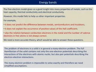
3-1-3. Metals, Semiconductors & Insulators • For electrons to experience acceleration in an applied electric field, they must be able to move into new energy states. This implies there must be empty states (allowed energy states which are not already occupied by electrons) available to the electrons. • The diamond structure is such that the valence band is completely filled with electrons at 0ºK and the conduction band is empty. There can be no charge transport within the valence band, since no empty states are available into which electrons can move.
3-1-3. Metals, Semiconductors & Insulators • The difference bet-ween insulators and semiconductor mat-erials lies in the size of the band gap Eg, which is much small-er in semiconductors than in insulators. Empty Empty Eg Eg Filled Filled Insulator Semiconductor
3-1-3. Metals, Semiconductors & Insulators • In metals the bands either overlap or are only partially filled. Thus electrons and empty energy states Overlap Metal are intermixed with-in the bands so that electrons can move freely under the infl-uence of an electric field. Partially Filled Filled Metal
3-1-4. Direct & Indirect Semiconductors • A single electron is assumed to travel through a perfectly periodic lattice. • The wave function of the electron is assumed to be in the form of a plane wave moving. • x : Direction of propagation • k : Propagation constant / Wave vector • : The space-dependent wave function for the electron
3-1-4. Direct & Indirect Semiconductors • U(kx,x): The function that modulates the wave function according to the periodically of the lattice. • Since the periodicity of most lattice is different in various directions, the (E,k) diagram must be plotted for the various crystal directions, and the full relationship between E and k is a complex surface which should be visualized in there dimensions.
3-1-4. Direct & Indirect Semiconductors E E Eg=hν Eg Et k k Direct Indirect Example 3-1
3-1-4. Direct & Indirect Semiconductors • Example 3-1: Assuming that U is constant in for an essentially free electron, show that the x-component of the electron momentum in the crystal is given by Example 3-2
3-1-4. Direct & Indirect Semiconductors • Answer: The result implies that (E,k) diagrams such as shown in previous figure can be considered plots of electron energy vs. momentum, with a scaling factor .
3-1-4. Direct & Indirect Semiconductors Properties of semiconductor materials • Si • Ge • GaAs • AlAs • Gap Eg(eV) n p Lattice Å 1.11 1350 480 2.5E5 D 5.43 0.67 3900 1900 43 D 5.66 1.43 8500 400 4E8 Z 5.65 2.16 180 0.1 Z 5.66 2.26 300 150 1 Z 5.45
L X L X 0.3eV X L 3-1-5. Variation of Energy Bands with Alloy Composition E 3.0 E 2.8 2.6 2.4 2.2 2.0 1.43eV 2.16eV 1.8 k 1.6 AlxGa1-xAs GaAs AlAs 1.4 0 0.2 0.4 0.6 0.8 1 X
3-2. Carriers in Semiconductors Ec Eg 300ºK 18ºK 11ºK 15ºK 14ºK 20ºK 19ºK 13ºK 17ºK 12ºK 16ºK 1ºK 4ºK 2ºK 3ºK 0ºK 10ºK 8ºK 7ºK 6ºK 5ºK 9ºK Ev Electron Hole Pair E P H
0 3-2-1. Electrons and Holes E -kj kj k j` j
3-2-2. Effective Mass • The electrons in a crystal are not free, but instead interact with the periodic potential of the lattice. • In applying the usual equations of electrodynamics to charge carriers in a solid, we must use altered values of particle mass. We named it Effective Mass.
3-2-2. Effective Mass • Example 3-2: Find the (E,k) relationship for a free electron and relate it to the electron mass. E k
3-2-2. Effective Mass • Answer: From Example 3-1, the electron momentum is:
3-2-2. Effective Mass • Answer (Continue): Most energy bands are close to parabolic at their minima (for conduction bands) or maxima (for valence bands). EC EV
E X L 1.43eV k 3-2-2. Effective Mass • The effective mass of an electron in a band with a given (E,k) relationship is given by • Remember that in GaAs:
3-2-2. Effective Mass • At k=0, the (E,k) relationship near the minimum is usually parabolic: • In a parabolic band, is constant. So, effective mass is constant. • Effective mass is a tensor quantity.
3-2-2. Effective Mass EV EC Table 3-1. Effective mass values for Ge, Si and GaAs. † m0 is the free electron rest mass.
A perfect semiconductor crystal with no impurities or lattice defects is called an Intrinsic semiconductor. In such material there are no charge carriers at 0ºK, since the valence band is filled with electrons and the conduction band is empty. 3-2-3. Intrinsic Material
Eg 3-2-3. Intrinsic Material e- Si h+ n=p=ni
3-2-3. Intrinsic Material • If we denote the generation rate of EHPs as and the recombination rate as equilibrium requires that: • Each of these rates is temperature depe-ndent. For example, increases when the temperature is raised.
3-2-4. Extrinsic Material • In addition to the intrinsic carriers generated thermally, it is possible to create carriers in semiconductors by purposely introducing impurities into the crystal. This process, called doping, is the most common technique for varying the conductivity of semiconductors. • When a crystal is doped such that the equilibrium carrier concentrations n0 and p0 are different from the intrinsic carrier concentration ni , the material is said to be extrinsic.
3-2-4. Extrinsic Material Ec Ed 50ºK 18ºK 20ºK 15ºK 14ºK 11ºK 19ºK 17ºK 13ºK 12ºK 16ºK 1ºK 4ºK 2ºK 3ºK 0ºK 10ºK 8ºK 7ºK 6ºK 5ºK 9ºK Ev Donor
3-2-4. Extrinsic Material Ec 50ºK 18ºK 20ºK 15ºK 14ºK 11ºK 19ºK 17ºK 13ºK 12ºK 16ºK 4ºK 1ºK 2ºK 3ºK 0ºK 10ºK 8ºK 7ºK 6ºK 5ºK 9ºK Ea Ev Acceptor
3-2-4. Extrinsic Material e- Sb h+ Al Si
3-2-4. Extrinsic Material • We can calculate the binding energy by using the Bohr model results, consider-ing the loosely bound electron as ranging about the tightly bound “core” electrons in a hydrogen-like orbit.
3-2-4. Extrinsic Material • Example 3-3: Calculate the approximate donor binding energy for Ge(εr=16, mn*=0.12m0).
3-2-4. Extrinsic Material • Answer: Thus the energy to excite the donor electron from n=1 state to the free state (n=∞) is ≈6meV.
3-2-4. Extrinsic Material • When a ш-Vmaterial is doped with Si or Ge, from column IV, these impurities are called amphoteric. • In Si, the intrinsic carrier concentration ni is about 1010cm-3 at room tempera-ture. If we dope Si with 1015 Sb Atoms/cm3, the conduction electron concentration changes by five order of magnitude.
3-2-5. Electrons and Holes in Quantum Wells • One of most useful applications of MBE or OMVPE growth of multilayer compou-nd semiconductors is the fact that a continuous single crystal can be grown in which adjacent layer have different band gaps. • A consequence of confining electrons and holes in a very thin layer is that
3-2-5. Electrons and Holes in Quantum Wells these particles behave according to the particle in a potential well problem. Al0.3Ga0.7As GaAs Al0.3Ga0.7As 50Å E1 0.28eV 1.85eV 1.43eV 1.43eV 0.14eV Eh
3-2-5. Electrons and Holes in Quantum Wells • Instead of having the continuum of states as described by , modified for effective mass and finite barrier height. • Similarly, the states in the valence band available for holes are restricted to discrete levels in the quantum well.
3-2-5. Electrons and Holes in Quantum Wells • An electron on one of the discrete condu-ction band states (E1) can make a transition to an empty discrete valance band state in the GaAs quantum well (such as Eh), giving off a photon of energy Eg+E1+Eh, greater than the GaAs band gap.
3-3. Carriers Concentrations • In calculating semiconductor electrical pro-perties and analyzing device behavior, it is often necessary to know the number of charge carriers per cm3in the material. The majority carrier concentration is usually obvious in heavily doped material, since one majority carrier is obtained for each impurity atom (for the standard doping impurities). The concentration of minority carriers is not obvious, however, nor is the temperature dependence of the carrier concentration.
3-3-1. The Fermi Level • Electrons in solids obey Fermi-Dirac statistics. • In the development of this type of statistics: • Indistinguishability of the electrons • Their wave nature • Pauli exclusion principle must be considered. • The distribution of electrons over a range of these statistical arguments is that the distrib-ution of electrons over a range of allowed energy levels at thermal equilibrium is
3-3-1. The Fermi Level k : Boltzmann’s constant f(E) : Fermi-Dirac distribution function Ef : Fermi level
f(E) 1 1/2 E Ef 3-3-1. The Fermi Level T=0ºK T1>0ºK T2>T1
f(Ec) [1-f(Ec)] 3-3-1. The Fermi Level E f(Ec) Ec Ef Ev ≈ ≈ f(E) Intrinsic p-type n-type 1 0 1/2