Download
1 / 1
10 likes | 109 Views
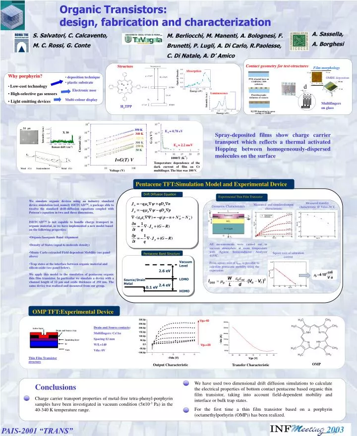
Structure. Vacuum level. N. N. H. H. N. N. = 3.4eV. = 4.8eV. Luminescence. Intensity (a.u.). PVD of metal layer on CORNING 7059 substrate. 0.7 eV. LUMO. Photolitographic definition of contacts. H 2 TPP. 2.0 eV. Energy (eV). E F. HOMO. 0.7 eV. 50 m m. -9. 10.

E N D
Structure Vacuum level N N H H N N = 3.4eV = 4.8eV Luminescence Intensity (a.u.) PVD of metal layer on CORNING 7059 substrate 0.7 eV LUMO Photolitographic definition of contacts H2TPP 2.0 eV Energy (eV) EF HOMO 0.7 eV 50 mm -9 10 350 K Absorption -10 10 340 K EA 0.78 eV 325 K Optical Density -11 10 300 K G (A V-1) 250 K -12 10 50 K EA 2.2 meV Energy (eV) -13 10 I=G(T) V 1000/T (K -11 -14 10 10 10 100 -12 Drift Diffusion Equation 10 -13 10 -14 10 5 10 15 20 25 -1 ) 2003 Organic Transistors: design, fabrication and characterization A. Sassella, A. Borghesi S. Salvatori, C. Calcavento, M. C. Rossi, G. Conte M. Berliocchi, M. Manenti, A. Bolognesi, F. Brunetti, P. Lugli, A. Di Carlo, R.Paolesse,C. Di Natale, A. D’ Amico Contact geometry for test-structures Film morphology 70 nm 10 mm OMBE deposition • Why porphyrin? • Low-cost technology • High-selective gas sensors • Light emitting devices • deposition technique • plastic substrate 0 5 150 nm 0 d 0 5 10 mm 10 mm Electronic nose 0 5 5 0 10 mm Multi-colour display Multifingers on glass Band diagram 1.4 1.6 1.8 2 2.2 H2TPP deposition by spray casting or OMBE Spray-deposited films show charge carrier transport which reflects athermal activated Hopping between homogeneously-dispersed molecules on the surface Intensity (a.u.) Current (A) Raman shift (cm-1) EF Va Temperature dependence of the dark current of film on Cr multifinger. The bias was 100 V. Metal (Cr) Semiconductor Metal (Cr) Voltage (V) Pentacene TFT:Simulation Model and Experimental Device Experimental Thin Film Transistor We simulate organic devices using an industry standard device simulation tool, namely ISETCADTM, a package able to resolve the standard drift-diffusion equations coupled with Poisson’s equation in two and three dimensions. Measured transfer characteristic @ Vds=-30 V Measured and simulatedoutput characteristic Geometric Characteristics • ISETCADTM is not capable to handle charge transport in organic material, so we have implemented a new model based on the following properties: • Organic/Inorganic Band Alignment • Density of States (equal to molecule density) • Monte Carlo extracted Field dependent Mobility (see panel above) • Trap states at the interface between organic material and silicon oxide (see panel below). All measurements were carried out in vacuum atmosphere at room temperature with Agilent Semiconductor Analyzer 4155C. Square root of saturation corrent Pentacene Band Structure Vacuum Level From square root of IDSS is possible to calculate pentacene mobility using the expression: 2.6 eV We apply this model to the simulation of pentacene organic thin film transistor. In particular we simulate a device with a channel length of 12 m and oxide thickness of 250 nm. The same device was realized and measured from our group. LOMO Source/Drain Metal 2.4 eV 0.1 eV HOMO OMP TFT:Experimental Device Drain and Source contacts: Multifingers: Cr/Au Spacing:12 mm W/L=140 Vth= 0V Active layer Drain and Source (Au) Insulating layer Si-- Gate Thin Film Transistor structure OMP Output Characteristic Transfer Characteristic We have used two dimensional drift diffusion simulations to calculate the electrical properties of bottom contact pentacene based organic thin film transistor, taking into account field-dependent mobility and interface or bulk trap states. For the first time a thin film transistor based on a porphyrin (octamethylporhyrin (OMP)) has been realized. Conclusions Charge carrier transport properties of metal-free tetra-phenyl-porphyrin samples have been investigated in vacuum condition (5x10⁻³ Pa) in the 40-340 K temperature range. PAIS-2001 “TRANS”