Download
1 / 14
140 likes | 269 Views
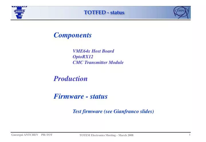
TOTFED - status. Components VME64x Host Board OptoRX12 CMC Transmitter Module Production Firmware - status Test firmware (see Gianfranco slides). TOTFED – Components. VME64x Host Board: - 9U VME64x Slave Module - Accepts several mezzanine modules

E N D
TOTFED - status Components VME64x Host Board OptoRX12 CMC Transmitter Module Production Firmware - status Test firmware (see Gianfranco slides)
TOTFED – Components • VME64x Host Board: • - 9U VME64x Slave Module • - Accepts several mezzanine modules • - Local Bus Master 32bits/40MHz; • - 18MB Spy Memory • OptoRX12: • - Custom 12 Channels Optical Receiver for GOH • - 12-channel digital optical receiver by NGK; • Altera Stratix GX EP2SGX60 device with embedded • hardware de-serializers for up to ~3.2Gbps; • - Connect via five 64pin connectors to the VME board; • - Has connectors for “CMC Transmitter” module • CMC Transmitter Module*: • - CMS DAQ Standard parallel data transfer module • - Using S-Link64 interface • * Not used in the beginning VME64x Host Board OptoRX12 CMC TR
Readout Crate TOTFED TOTFED TOTFED CAEN TTCci FEC TOTFED in Readout System • TOTFED is set of: • “VME64x Host Board”; • 3 x “OptoRX12” modules; • 3 x “CMC Transmitter” modules • - 2 x “Optional” modules • TOTFED in the Readout Crate
TOTFED – status - Produced 6 boards prototype V1: - 2 in CMS-ES; - 1 in 555 Lab; - 1 in Pisa; - 2 in my office – 1 for tests + 1 with partial soldiering problems - Continue tests on the board; - Second version EDA-01349-V2 on EDMS; - Preparation for final production – PCB TECH - Israel: - 5 boards pre-series in production – expecting soon; - 90 boards (i.e. 65 boards for ES-CMS, 25 boards for TOTEM); - Board Test Bench - in progress - New in the firmware development: - JTAG via VME code - developed, to be implemented; - I2C code to TTCrx - developed, implemented; - Unique Serial Number code - developed, implemented; - Test Firmware - developed, implemented
Spy 4 Memory 192bits 64bits OpRX 1 + S-Link64 32bits VME64x Interface 32bits MAIN 1 16bits USB 1 Spy 1 Memory JTAG VME64x OpRX 1 + S-Link64 Merger FPGA Local Bus 32bits MAIN 2 16bits USB 2 Buffers Spy 2 Memory 64bits OpRX 1 + S-Link64 To S-Link64 32bits MAIN 3 16bits USB 3 CCS/TTS Spy 3 Memory Local Bus Optional 16bits CLOCK USB 4 TTCrx QPLL CLOCK TOTFED – Block Diagram Paper on TWEPP07 workshop - link 5
“VME64x Controller” (1) • Specification - link • Implemented in ALTERA Cyclone EP1C4F400C8N using Quartus II 7.2 tools • Blocks: • - VME Main Controller • - VME64x complaint device • - Primary Local Bus Controller • - 32bit Data, 20 bit Address and Control • - Secondary Local Bus Controller • - 32bit Data/Address Multiplexed and Control • - used for optional MFEC module • - FPGAs Page Reload interface • - JTAG Controller • - From VME64 bus for remote programming • - Trigger Timing Control (TTC) interface • - Trigger Throttling System (TTS) interface • - I2C Interface for TTCrx chip control; • - JTAG Controller
“VME64x Controller” (2) Hierarchical Design: Entry using schematics, block diagrams, AHDL, VHDL, and Verilog HDL;
“MAIN Controller” and “MERGER Controller” (1) • Specification – in preparation • Implemented in ALTERA Stratix EP1S20F780 using Quartus II 7.2 tools • Blocks: • - INPUT SPY Buffer • - Parallel 192 bit @ 40 MHz SPY Data Buffer • - MEMORY Interface Controller • - Flow-Through SRAM 18-Mbit (512K x 36) with NoBL • - 3 chips for 96bit Data @ 80MHz • - Local Bus Interface • - 32bit Data, 20 bit Address and Control • - USB 2.0 Interface controller • - High-Speed USB Interface Device CY7C68001 chip • - Interconnect Bus • - 64 bit between every MAIN Controller and MERGER Controller • - Trigger Throttling System (TTS) interface • - S-Link64 Interface Controller (for MERGER only) • - 64bit Parallel Data Bus and Control on P2 connector
“OptoRX12 Controller” • Designed by “CMS-ES” group • Implemented in ALTERA Stratix II GX family • Blocks: • - Embedded Hardware De-serializers for data - up to ~3.2Gbps • - Gigabit Ethernet protocol/encoding • - 12 channels • - Input Data Buffers • - 3 FIFO’s per group of 4 optical channels • - Output Data Interface • - Parallel 192 bit @ 40 MHz to MAIN • - S-Link64 Interface • - 64bit Parallel Data Bus and Control on top connectors • - Trigger Timing Control (TTC) interface • - Event Builder (in S-Link64 output) • - Data transfer to MAIN and to the MERGER Controllers
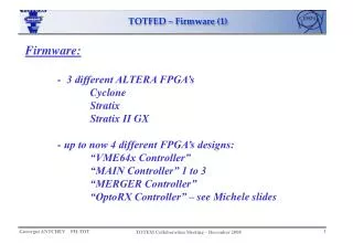
FPGA’s Summary • 3 different ALTERA FPGA’s • Cyclone • Stratix • Stratix II GX • 4 different FPGA’s design • “VME64x Controller” • “MAIN Controller” 1 to 3 • “MERGER Controller” • “OptoRX Controller” • Designs Status • Exist versions of all FPGA’s designs • Basic blocks were designed before the board layout (for pin assignment reason) • More functions to be implemented • Temp. control one wire interface • MAIN Controller arbiter • Event Builder in OptoRX12 • Test remaining functionalities • Data path - OptoRX + S-Link64 + MAIN + VME or USB
Test Firmware • OptoRX: • firmware development: • emulation of the VFAT • streaming data • Two kind of outputs: • to the S_link (64 bit) • to the Main FPGA (192 bit) 192 FIFO FULL • Main: • firmware development: • management of data coming • from OptoRX • output: 32 bit every clock cycle on the • Local Bus • Main FPGA sends to OptoRX a signal to • stop transmitting data
Timing simulation • OptoRX: • Main:
Conclusions TOTFED - V2 in pre-series production; - All components ready for final production Firmware: - Progress has been made in all (FPGA’s) building blocks Documentation: - Specifications on draft - Web page in preparation