Download
1 / 9
90 likes | 199 Views
VFE/MGPA considerations for EE/VPT. EB/EE electrical spec. differences: full-scale signal noise input capacitance dominated by: APD capacitance (x2) for barrel VPT -> MGPA interconnect for end-cap MGPA suits barrel and endcap full-scale signal

E N D
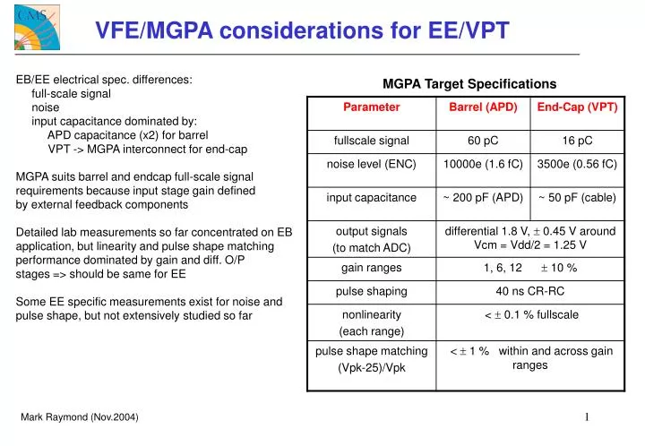
VFE/MGPA considerations for EE/VPT EB/EE electrical spec. differences: full-scale signal noise input capacitance dominated by: APD capacitance (x2) for barrel VPT -> MGPA interconnect for end-cap MGPA suits barrel and endcap full-scale signal requirements because input stage gain defined by external feedback components Detailed lab measurements so far concentrated on EB application, but linearity and pulse shape matching performance dominated by gain and diff. O/P stages => should be same for EE Some EE specific measurements exist for noise and pulse shape, but not extensively studied so far MGPA Target Specifications Mark Raymond (Nov.2004)
MGPA Architecture input stage CF chosen for max. poss. gain depending on barrel/end-cap RF chosen for 40 ns decay avoids pile-up CFRF external components => 1 chip suits barrel & end-cap CF//RF = 39pF//1k (barrel) = 8p2//4k7 (endcap) differential current O/P stages external termination 2RICI = 40 nsec. => low pass filtering on all noise sources within chip 3 gain channels 1:6:12 set by resistors (on-chip), for linearity, feeding common- gate stages i I2C and offset generator RI CI i VCM RG1 RI i DAC RI CI VCM RG2 RI ext. trig. CCAL input stage charge amp. RI CI VCM RG3 I/P RI diff. O/P stages gain stages RF CF RFCF VCM
Noise Sources common-gate gain stage vRf input stage Rf diff. output stage source follower Cf iCG RG vFET CIN iRG input stage high Cf (low gain) to cope with large full-scale signals => corresponding low Rf for 40 ns time const. => Rf noise dominates over input FET gain stage contribution can’t avoid for low gain range (RG big) but this range only used for larger signals so signal/noise still acceptable hand calculation these values calculated for CF//RF = 39pF//1k (barrel) CF//RF = 12pF//3k3 (endcap) (vFET ~ 0.23 nV/(Hz)1/2 )
Choice of 1st stage feedback components depends on fullscale signal requirement (VPT response and dynamic range requirement) barrel case values normalised to 60 pC barrel fullscale
Noise Measurement (VFE card) BARREL (CF//RF = 39pF//1k) END-CAP (CF//RF = 8p2//4k7) high gain chan. mid gain chan. high gain chan. mid gain chan. ENC [rms electrons] 7240+5.8/pF 7870+4.9/pF 3040+4.5/pF 3270+4.5/pF added capacitance [pF] added capacitance [pF] weak dependence on input capacitance as expected within spec. for high and mid-gain ranges: barrel < 10000 e, end-cap < 3500 e low gain range: barrel: 27300 e ± 12% end-cap: 8200 e ± 11% completely dominated by gain stage noise but signals large => electronic noise not significant (< 0.2% contribution to overall barrel energy res’n.)
End-cap signal simulation CSA O/P End-cap VPT interface coax without coax I(t) Cdet MGPA with coax I(t) current source with 10 ns decay time Cdet = 5 pF (2 pF + stray) coax = RG 179 (thin 50 ohm) 75 cm long some ringing observable at input stage O/P smoothed out at chip O/P chip O/P without coax with coax previously presented at design review (Jan.2003)
Measurement 2 pF 80 cm. thin 50 W coax MGPA pulse shapes at chip O/P high gain range ~ ¾ fullscale signal
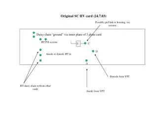
Specific EE issues coax MGPA input protection on-chip protection not sufficent to withstand VPT breakdown (RAL measurements already proved) => additional external protection diode => extra capacitance (~ few 10’s pF shouldn’t be a problem) => prot. diode rad-hardness issues more remote opto-electric transducer => transmission line effects => grounding/shielding issues HV filter card diagram - courtesy Claire Shepherd-Themistocleous