Download
1 / 34
340 likes | 476 Views
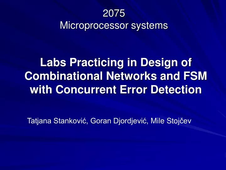
2075 Microprocessor systems. Labs Practicing in Design of Combinational Networks and FSM with Concurrent Error Detection. Tatjana Stanković , Goran Djordjević , Mile Stoj čev. Outline of the talk. I. Introduction II. Review of the Exercises III. Tutorial Content

E N D
2075Microprocessor systems Labs Practicing in Design of Combinational Networks and FSM with Concurrent Error Detection Tatjana Stanković, Goran Djordjević, Mile Stojčev
Outline of the talk I. Introduction II. Review of the Exercises III. Tutorial Content IV. Description of Overall Design Procedure V. Examples of VHDL synthesis VI. Concurrent error detection VII. Conclusion
2075Microprocessor systems • Directions: • Electronics, • Communications, • Microelectronics • VII semester 2+2+1 • VIII semester 2+2+1
Outline of the talk I. Introduction II. Review of the Exercises III. Tutorial Content IV. Description of Overall Design Procedure V. Examples of VHDL synthesis VI. Concurrent error detection VII. Conclusion
2075Microprocessor systems Structure of Lab Exercises Lab exercises Programming oriented Logic design oriented DOS (4 exercises) VHDL description of three stage pipelined system Intel 80x86 (15 exercises) Four more exercises about VHDL design of logic structure with concurrent error detection MIPS (5 exercises)
2075Microprocessor systems What we propose? Involving four additional exercises in logic design to cover the following topics: • CAD tools for logic design • Design of combinational networks with concurrent error detection with examples • Design of sequentional networks with concurrent error detection with examples
2075Microprocessor systems What kind of literature use students? • Tutorial for VHDL design • Textbook for Digital Logic Design
2075Microprocessor systems Outline of the talk I. Introduction II. Review of the Exercises III. Tutorial Content IV. Description of Overall Design Procedure V. Examples of VHDL synthesis VI. Concurrent error detection VII. Conclusion
2075Microprocessor systems Tutorial Content • General Introduction • VHDL for Synthesis After passing this step students become familiar with writing and simulating VHDL code, modeling combinational and sequential circuits, using design hierarchy. • CAD tools and Design Flow During this step students learn how to use CAD tool for designing logic structures with PLD circuits.
2075Microprocessor systems Outline of the talk I. Introduction II. Review of the Exercises III. Tutorial Content IV. Description of Overall Design Procedure V. Examples of VHDL synthesis VI. Concurrent error detection VII. Conclusion
2075Microprocessor systems Description of the Overall Design Procedure • Design entry • Design synthesis • Functional simulation • Design implementation
CAD system Xilinx Integrated Software Environment - ISE 5 for design entry, synthesis and physical implementation for FPGA circuits ModelSim XE II/Starter 5.7 for functional and timing VHDL simulation.
Design flow ModelSim ISE
Design entry - writing source code in VHDL - behavioral description
Design synthesis Synthesis Report Synthesis is process of generating a logic circuit from a formal circuit description, automatically. This process translate, or compile, VHDL code into a network of logic gates.
Functional simulation Test bench Simulation output
Design implementation Post-Place & Route Static Timing Report Floor Planner
2075Microprocessor systems Outline of the talk I. Introduction II. Review of the Exercises III. Tutorial Content IV. Description of Overall Design Procedure V. Examples of VHDL synthesis VI. Concurrent error detection VII. Conclusion
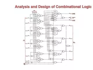
VHDL synthesis of combinational circuits Four ways to describe a MUX– behavioral description If-then-else statement select statement case statement conditional assignment
Arithmetic circuits Ripple-carry adder – structural description
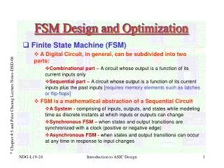
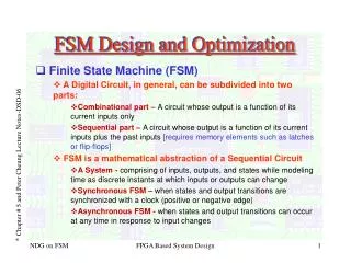
VHDL synthesis of sequential circuitsFSM code template - layout combinational next state and output logic The correct model is one in which the sequential current state logic has been separate from the combinational next state and output logic. sequential current state logic
VHDL synthesis of sequential circuitsFSM state encoding Source code using sequential state encoding: Coding schemes (sequential, Gray, Johnson, and one-hot) are defined in separate package:
2075Microprocessor systems Outline of the talk I. Introduction II. Review of the Exercises III. Tutorial Content IV. Description of Overall Design Procedure V. Examples of VHDL synthesis VI. Concurrent error detection VII. Conclusion
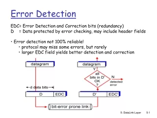
Concurrent error detectionWhy it is important? Technological advances have increased drastically the complexity of integrated circuits that can be realized on a single chip. The move towards VLSI technologies with higher frequencies, lower voltage levels, and smaller noise margins is increasing the susceptibility of systems to transient and intermittent faults. Early detection of errors is crucial for preserving the state of the system and maintaining data integrity. Techniques for concurrent error detection (CED) permit early detection and containment of errors before they can propagate to other parts of the system and corrupt data.
General structure of CED One general approach for CED is to encode the outputs of a circuit with an error detecting code.
The insertion of CED circuitry We use a methodology for insertion of CED in synthesizable VHDL description of the original circuit, at the front-end of the synthesis process. This methodology has several advantages: • It allows the error detection circuitry to be optimized along with the functional circuitry. • The CED circuitry is taken into account when satisfying timing constraints. • The approach of inserting the CED circuitry can be easily and seamlessly incorporated into the standard design flow.
Techniques for CED The techniques for CED depend on the way in which the output of functional logic is encoded. We use: • duplication function • parity codes • Berger codes • Bose-Lin codes All mentioned techniques can be applied on the outputs of the combinational circuits or on the states of sequential circuit.
Duplication of function as a technique for CED The design implements two copies of the same circuit. The second copy produces output values complementing the value of the first copy, and a tree of two-rail code (TRC) checkers makes a bitwise comparison of the outputs.
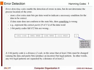
Parity codes as a technique for CED The parity bit is equal to the sum modulo 2 of the information bits or their complements. A parity check code is a code in which each check bit is a parity check for a group of output bits.
Berger and Bose-Lin codes as a technique for CED The Berger check symbol of the information can adopt either the binary representation of the number of zeros in the information (B0) or the ones complement of the number of ones in the information (B1). Bose-Lin codes - similar to Berger codes, but the number of bits is performed modulo 2, 4, 8 etc.
Layout of Lab Exercise for Combinational Networks with CED Original circuit Check symbol generator Check symbol generator is described as a separate process which include: - VHDL code of the original circuit - Code that transforms circuit outputs into check symbol bits
Layout of Lab Exercise for Combinational Networks with CED Checker Structural description of circuit with CED hardware
FSM with CED Parity bits technique The simplest technique for inserting CED in FSM is to append a parity bit to each state-codeword.
Conclusion Extension of Lab exercises for course Microprocessor Systems is considered with goal to include VHDL synthesis of combinational and sequential networks with concurrent error detection using contemporary CAD tools.