Download
1 / 13
141 likes | 570 Views
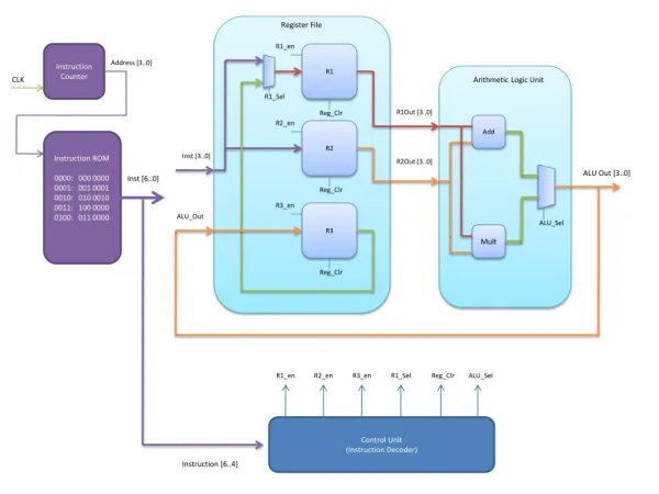
4 BIT Arithmetic And Logic Unit (ALU) Philips 74HC/HCT181. Brijesh Chavda Meet Aghera Mrugesh Chandarana Sandip Patel Adviser David Parent Date: 12/03/05. Abstract. Goal is to design 4-bit ALU driving up to 25fF. Perform arithmetic operations like A+B, A+B’, A-1, A+(AB’), AB-1.

E N D
4 BIT Arithmetic And Logic Unit (ALU)Philips 74HC/HCT181 Brijesh Chavda Meet Aghera Mrugesh Chandarana Sandip Patel Adviser David Parent Date: 12/03/05
Abstract • Goal is to design 4-bit ALU driving up to 25fF. • Perform arithmetic operations like A+B, A+B’, A-1, A+(AB’), AB-1. • Perform Logical operations like Ex-OR, Compare, AND, NAND, NOR, OR plus 10 other logic operations. • The data must be transferred at clock rate of 200MHz. • Maximum area is 323 X 760 µm².
Introduction • ALU is a building block of several complex circuits. • The designed ALU is able to handle two 4 bit inputs to produce required output based on the output selector lines. • Challenging to design 16 logic level circuit working with 5ns delay. • Using this knowledge and experience, we can move on to designing more complex integrated circuits.
Design Flows • Calculate the longest path delay from the circuit. • Create schematic and layout for INV, NAND2 and NAND3. • Combine these three building blocks to create the different blocks of the circuit. • Test the schematic logic of all the modules. • Assembled all the modules and flip-flops. • Run DRC, extracted and LVS check to verify the design. • Analyze the circuit power and timing using Analog Affirma.
Lesson learned • Follow the steps and guideline given by Dr. Parent • How to design a compact circuit. • How to fix the LVS errors. • Optimize transistor size to meet out specifications. • How to use cadence tools.
Acknowledgements • Thanks to Professor David Parent for his guidelines and help throughout the project. • Thanks to Cadence Design Systems for VLSI Lab.