Download
1 / 10
100 likes | 207 Views
CCD-based Vertex Detector. CCD-based Vertex Detector - LCFI status report Konstantin Stefanov RAL Conceptual design and goals Detector R&D program at LCFI Development of Column Parallel CCDs and readout electronics Thin ladder program for mechanical support of the sensors Summary.

E N D
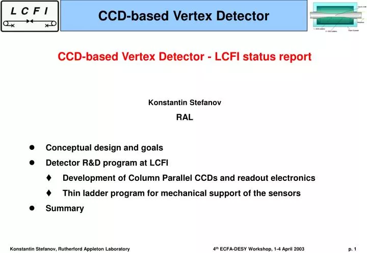
CCD-based Vertex Detector CCD-based Vertex Detector - LCFI status report Konstantin Stefanov RAL • Conceptual design and goals • Detector R&D program at LCFI • Development of Column Parallel CCDs and readout electronics • Thin ladder program for mechanical support of the sensors • Summary
Conceptual Design and Goals 5 layers at radii 15, 26, 37, 48 and 60 mm; Low power, gas cooled; High precision, low mass support mechanics; Encased in light foam cryostat; Minimum number of external connections. Thin detector (< 0.1% X0) for low error from multiple scattering; Close to the interaction point for reduced extrapolation error; Readout time: 8 ms for NLC/JLC (read between trains) 50 μs for TESLA inner layer (read 20 times during the train); Pixel size 20 μm20 μm, stand-alone tracking, radiation hard, etc.
CCD Development Large area, high speed CCDs • Inner layer CCDs: 10013 mm2, 2500(V)650(H) pixels per CCD end; • Outer layers: 2 CCDs with size 12522 mm2 , 6250(V)1100(H) pixels; • 120 CCDs, 799106 pixels (20 μm square) in total; • For NLC/JLC: readout time 8 ms in principle sufficient, but not easy to achieve with standard CCDs, Column Parallel CCD is desirable; • For TESLA: • 50 μs readout time for inner layer CCDs : 50 Mpix/s from each CCD column • Outer layers: 250 μs readout, 25 MHz from each column • Column Parallel CCD is essential • Satisfy TESLA requirements, but thinking about NLC/JLC as well • CPCCD for JLC/NLC could be very advantageous
CCD Ladder End • Electronics only at the ends of the ladders; • Bump-bonded assembly between thinned CPCCD and readout chip; • Readout chip does all the data processing: • Amplifier and ADC with Correlated Double Sampling for each CCD column • Gain equalisation between columns • Hit cluster finding • Data sparsification • Memory and I/O interface • CPCCD is driven with high frequency, low voltage clocks; • Low inductance layout for clock delivery.
CCD Development CPCCDs for TESLA: • Quality of 50 MHz clocks over the entire device (area = 13 cm2): • Power dissipation: • Large capacitive load (normally 2-3 nF/cm2), needs low clock amplitudes; • Low average power ( 10 W) for the whole detector, but large peak power (TESLA duty cycle = 0.5%). • Feedthrough effects: • 2-phase drive with sine clocks – natural choice because of symmetry and low harmonics • Ground currents and capacitive feedthrough largely cancel CPCCDs for NLC/JLC: • Low readout frequency (780 kHz) – in principle few electrons noise could be achieved;
Our First CPCCD Delivered, testing imminent Direct connections and 2-stage source followers Two phase, pixel size 20 μm 20 μm; Wire/bump bond connections to readout chip and external electronics; Two charge transport regions; Serious testing in the following months! 1-stage source followers and direct connections on 20 μm pitch
Readout Chip Design Wire/bump bond pads Voltage Amplifiers Charge Amplifiers 250 5-bit flash ADCs FIFO Wire/bump bond pads First bump-bondable readout chip (CPR-1) to be delivered in a few weeks • Designed by the Microelectronics Group at RAL; • Voltage amplifiers for the 1-stage SF outputs, charge amplifiers for the direct connections; • Everything on 20 μm pitch; • 0.25 μm CMOS process; scalable and designed to work at 50 MHz; • Smaller chip with ADC arrays and amplifiers already tested; • Work on next generation chip with 22 cluster finding and sparsification has started.
Thin Ladder R&D A program to design CCD support structures with the following properties: • Very low mass (< 0.4% X0– SLD VXD3) • Shape repeatability to few microns when temperature cycled down to –100 C; • Compatible with bump bonding; • Overall assembly sufficiently robust for safe handling with appropriate jigs; Three options: • Unsupported CCDs – thinned to 50 μm and held under tension • Semi-supported CCDs – thinned to 20 μm and attached to thin (and not rigid) support, held under tension; • Fully-supported CCDs – thinned to 20 μm and bonded to 3D rigid substrate (e.g. Be)
Semi-supported Option Beryllium substrate with adhesive balls Thinned CCD ( 20 μm) CCD brought down Shims Adhesive Assembly after shim removal and curing 0.2mm Beryllium substrate (250 μm) 1 mm FEA simulations continuing: • Distortions of only few μm, optimise adhesive pitch and size; • Silicone adhesive: NuSil, excellent at low temperature • Layer thickness 0.12% X0 XY stage for 2-dimensional profiling being assembled: • Laser displacement meter • Resolution 1 μm • Models made from steel + unprocessed Si will be measured
Summary • Detector R&D work at the LCFI collaboration: • Development of fast column parallel CCD and its readout chip; • Precision mechanical support of thinned CCDs. • Most aspects of the R&D are applicable to all proposed LC machines; • High speed CPCCDs are mainly for TESLA, however NLC/JLC likely to benefit from slow CPCCDs; • Significant work is required, challenging combination of chip size and speed; • More results to follow in a couple of months. More information is available from the LCFI’s web page: http://hep.ph.liv.ac.uk/~green/lcfi/home.html