Download
1 / 26
260 likes | 381 Views
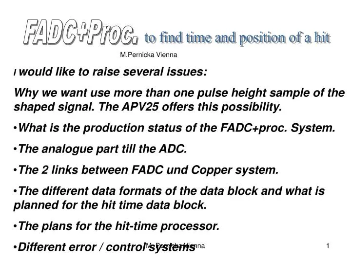
FADC+Proc. to find time and position of a hit. M.Pernicka Vienna. I would like to raise several issues: Why we want use more than one pulse height sample of the shaped signal. The APV25 offers this possibility. What is the production status of the FADC+proc. System.

E N D
FADC+Proc. to find time and position of a hit M.Pernicka Vienna • I would like to raise several issues: • Why we want use more than one pulse height sample of the shaped signal. The APV25 offers this possibility. • What is the production status of the FADC+proc. System. • The analogue part till the ADC. • The 2 links between FADC und Copper system. • The different data formats of the data block and what is planned for the hit time data block. • The plans for the hit-time processor. • Different error / control systems M. Pernicka Vienna
The point of storing a signal has a certain jitter. The Trigger is synchronised with the clock for the APV25 ( for a LHC experiment no problem) The trigger itself has a time jitter Therefore 3 samples around the maximum would be a great advantage ( or necessary ) The APV25 has this facility. ~60 ns M. Pernicka Vienna
The trigger can have a jitter more than the shaping time and the occupancy is still too big. To increase the shaping time would be the wrong solution! Therefore we will measure the time of each signal to the trigger and each other! We use the 3 highest samples to calculate the time. An RMS of 2 ns was obtained (with high S/N) in various beam tests. We have to live with jitter and latency of the trigger, we have to optimise the shaping time and clock frequency (and number samples) 6 samples are foreseen … max +/-50 ns trigger jitter can be handled. M. Pernicka Vienna
With 6 time sample we can calculate the time in a range of 4 clock width M. Pernicka Vienna
The amount of data would be for every input n*140 data ( n=1,3,6,..) The answer was an FADC + processor module with 16 inputs and with a data processor for every input for position and time calculation. Every processing is a part of a pipeline. The limit of the trigger rate depends on the final design and could be as high as the trigger rate for the APV25. The ``mother´´ of this module is the readout module for the CMS pixel detector with 36 optical inputs. 2 other versions are used for the CMS beam conditions monitor system. M. Pernicka Vienna
2 BELLE_FADC+proc. module are ready(without the facility of time calculation) Mezzanine board From every Altera 9 transmission lines to P2 Data bus Control bus temporary M. Pernicka Vienna
Some remarks on the task of the APV-FADC-Processor system Main aims: You need output data of the ADC ( transparent mode ), to calculate ADC clock delay to the main clock, pedestal and threshold. An external gate signal is used as write signal of the ADC data in the memory and create on the control module a trigger and cal signal to the APVs Done by the VME system crate processor. To get the hit information after reorder and 2-pass common mode correction. To build for every hit 6 time samples. That means 6 times more data for one hit. The hit-time calculator reduces it to one. (Not included yet.) (To include neighbours in space above pedestal and under threshold. Again more data.) To get for every hit data the time. We will use the 3 time information from 6 time samples around the max. to find the time of the hit. (Neighbours in space can be included). In an unclear situation like 2 max are found, no max is found because max outside of the 6 time samples or shaping curve do not fit in the expected one, the full information, that means 6 time blocks are transmitted for further processing. That would increase the data amount but without any loss of information. A lot of test facilities for testing the different data processors are fore seen. M. Pernicka, H. Steininger M. Pernicka Vienna
Test pulse generator, 3 channel DAC, can create hit data Voltage Regulator + 1 V ALTERA daughter board for 4 inputs 4 channel input ADC daughter card DAC to adjust the offset of the incoming signal Buffer amplifier to add offset and input signal 4 input 10bit 100 MHz ADC, 4 clocks can be adjusted in steps of 0.5ns 4 inputs like SVD-2 FADC RJ 45 Analog equalizer (parameter: length of cable) gain adjustment M. Pernicka Vienna
The use of bit 31 – 0 for the different data types decided by VME command * With or with out neighbours Transpa rent data need strobe OR OR* Input header yes/no Main header always Hit + transp. Date, test Main Trailer always Hit + time date Inp Trailer yes/no Hit date 31=type of trailer =1 31=1 30-27 quality of data, type 31 type header = 0 30-27 trigger type/4 ??? 25-23 type of data / 3 16-31 CRC checksum 31typ of header =1 31-23 Transpar. Data after reorder need a window sig 31-23=0 transparent data belong to the hit 31-23 transp data ADC, some times or cont. date 0 Finesse 29-23 event number from input. 26-23 Time of hit 22-20 time block 1bis6 22-20 time block 1bis6 22-20 time max 1 bis5 20-16 time of clock/ trig include later Alt-C 0 7 19-16 input = 4 19-16 input = 4 19-16 input = 4 19-16 input = 4 19-16 input = 4 14,15 crate ? 13-9 module n Alt-C 15-9 Ped Correction-2 7 15-9 position 7 may be module error bits ? 15-9 position 7 15-9 position 7 may be input error bits 8 – 0 Transparent data 8-0 Pulse height data 8-0 Pulse height data 8-0 Pulse height data 8-0 Ped Correction-1 7-0 Event number, from Copper syst. / M. Pernicka Vienna The final aim *
The use of bit 31 – 0 for the different data types Main header always, for one module information Main header always Every input has its header, can be switched off by VME Input header yes/no 31 type header = 0 30-27 trigger type/4 25-23 type of data Module input header 31typ of header =1 Input header ? ? 29-23 event number from input. Input number counting the arriving header APV25 20-16 time of clock/ trig include later Alt-C Time between trigger and clock bus-data 0 Code N U 19-16 input = 4 16 inputs on module exists 14,15 crate ? 13-9 module n Alt-C Has to be included by VME Correction for the second common mode correction, can be + or - Correction factor for the first common mode correction, can be + or - 15-9 Ped Correction-2 7 Bus- signal from controller 7-0 Event number, from Copper syst. 8-0 Ped Correction-1 M. Pernicka Vienna *
From a single hit position and time block information Transpa rent data need strobe Need a trigger signal from the controller (Neco) and a strobe signal (bus) to collect APV25 data. Will be used by VME system Hit date 31-23=0 transparent data belong to the hit Transparent data which belong to the hit, still not included 31-23 Transpar. Data after reorder need a window sig Transparent data from input n after reorder. Input number+1 22-20 time block 1bis6 Number of the time block, at the moment 6 Code NU 7 19-16 input = 4 19-16 input = 4 Input 15-9 position 7 An APV25 has 128 signal outputs Each signal above a threshold in o0ne of the 6 time blocks 8-0 Pulse height data Transparent data from input one 8 – 0 Transparent data M. Pernicka Vienna
Hit + transp. Date, test Hit + time date The hit data are read out by finesse and spy memory, (VME) and the transparent data from one input and one time block with reduced frequency 1/256 under control from VME The final data for a hit with position and time 31=1 30-27 quality of data, type 31-23 transp data ADC, some times or cont. date 0 Still open 26-23 Time of hit 22-20 time block 1bis6 At the moment 6 19-16 input = 4 Time of the hit to the leading edge of clock 19-16 input = 4 15-9 position 7 15-9 position 7 Standard hit information Standard hit information 8-0 Pulse height data 8-0 Pulse height data M. Pernicka Vienna
Main Trailer always The end of a data block of the 16 oinputs 16-31 CRC checksum CRC16 (Cyclic Redundancy Check) may be module error bits ? The kind and use of `` errors ``are still open M. Pernicka Vienna
The use of the bit 68-64 bits on FADC board bus system and for the data link to FINESSE Input header Main header always Input Trailer Dummy Data Control bits for finesse Main trailer Yes/no 0 On connector 1 0 0 1 1 0 1 0 0 1 stop-bit 0 1 / 0 1 0 / 1 67 66 65 64 Head Trailer Stop Da En 0 HEADER 37/85 1 1 TRAILER 39/87 0 HALF_EV 38/86 0 DA_EN 36/84 0 1 M. Pernicka Vienna
Mezzanine board for BELLE FADC+proc 96 Pin Data 32 Data bus XD_0=bis XD_31 4 control lines DA_EN, HALF_EV, TRAILER.HEADER DCLK clock 40 MHz BSYFD busy Finesse 2 spares P - 3 P – 3 DC/DC + 5 V/ -5 Volt . . . 50 pin conector ADCRST;TRG; SCK, TAG0-7, TYP0, / TYP1-3 will be included in new version . . ADCBSY (BUSY), ADC_ERR (ERROR1_CON), SPARE1_WR_CON (or data) . . 2 spares . For the module busy ADCBSY (BUSY_COM ) All TW control lines are also bus lines later. At the begin a connector with 50 pins is used for the distribution of the control signals, now we use the P3 bus. . M. Pernicka Vienna
The 3 steps of FIFO’s for normal 6 time one hit information read out time calculation for 16 inputs at 20 % occupancy Pipe line • Data • 21µs 154 3,85 µs proc FIFO-1 2K Altera_N proc 154 3,85 µs proc FIFO-2 16K*72 616 data 15,4 µs proc 32 ( 64 ) bit bus 40 MHz • Data • 21ys 154 3,85 µs Pipe line proc FIFO-1 2K FIFO-3 Final data block Main memory spy memory Error calculator 31µs To finesse proc ~62µs 154 3,85 µs 31µs proc 40 MHz 32 + 4 bit ~15K trigger Altera_Nc M. Pernicka Vienna proc
The 3 steps of FIFO’s for hit with time information read out 840*25ns= 21 µs All data are stored +hitinf Hit processor 8 bit +1 768 data 19.2 µs FIFO-1 2K Altera_N Only One FIFO-2 16K*72 64 bit 40 MHz (80Mhz) bus this bus limit mainly the trigger rate Hit time processing Strip data with one max or not Time calculation on board other vice out side FIFO-1 2K < 40 µs 20µs Between < 80µs < 20 µs <40 µs 20µs Altera_Nc M. Pernicka Vienna Sec. half
The 3 steps of FIFO’s for hit with time information read out 768 840*25ns= 21 µs Final hit data No time Hit processor Altera_N Time calculator for 4 inputs FIFO for final hit-data with time 64 bit = 2 hit data 40 MHz (80Mhz) bus Final hit data No time Hit processor Time calculator for 4 inputs Data 32+4 bit 40 MHz Final data block and FIFO Altera_Nc M. Pernicka Vienna Sec. half
A, A single hit, time calculated by `` Look up table ´´ or … • B, Max high of shaped pulse at the boundary above a certain value, will be used when necessary, time window 150 ns, but without time information or may be value 0 and 150 ns and marker bit. • C, 2 max. time information's are found, between a smaller sample, the time has to be found outside, may be together with CSC det. data. Marker bit included. • D Only one max. time info but the pulse shape do not fit in the expected shaping curve. Detected l in the `` Look up table´´. Final calculation out side. • E 2 real max – 2 times – but can only handled outside • F, small pulses, inside, hit pulse high information but time critical, marked Look up table decide outside Type of events A B C D E Ti me T T+1 T+2 T+3 T+4 T+5 Decision logic 512 strips = 4 APV….………1 M. Pernicka Vienna A strip cluster
Slow read in Every 6 clocks data from 4 inputs are read in. Data with and with out hit bit 4 FIFO + 24 Dual Port memories (128*9 bit) to transfer data format for processing time 194 exist Input 4 3 2 1 FIFO 128*9 Fast read out 128- N+3 1 128 N+2 1 128 N+1 1 128 N 1 output numb on APV 512 385 384 257 256 129 128 1 Si strip number Enable Time-x ns 512 Output data every strip data has up to 6 pulse height information's= One strip with 6 times readout time 4*128*25ns 128- N+3 1 128 N+2 1 128 N+1 1 128 N 1 512 385 384 257 256 129 128 1 Enable Time-x+25ns 128- N+3 1 128 N+2 1 128 N+1 1 128 N 1 512 385 384 257 256 129 128 1 Enable Time-x+125 ns Demux 2^7, 2^8 = enable memmory 1-128, 129-256,..385-512 Address 2^0 2^6 Address bits 2^0 -- 2^8 M. Pernicka Vienna
A possibility to realise hit time processing for 4 inputs = 4 APV25 (one detector) 2 hits, 2 max Which type of data: one max. can be processed, result or proc. outside Max. on the bounder proc. Outside rest proc. outside 1 hit in the time window 1 hit on the bounder Time x Raw time Time x+25 From 6 data use the 3 highest Fine time Time x+50 Single hit M U x Look up table DAQ Not foundtime Time x+75 Data <limit 6 data Time x+100 Hit data processing was not possible 6*8(9) bit data for one strip with marker has to be transferred, can be processed outside Reason: Pil up, multi trig. Data with 2 max Time x+125 Stop read 6*128 FIFO address=stripe position M. Pernicka Vienna
One of several possibilities to measure the time under evaluation ( The pedestal value of the signal should be for the Look Up Tables alwas the same ) Selects the 3 highes neiboughs The first 2 time inf.<9bitg the 3. <8 bit Coarse time 0,25,50,75ns 2Bit S T1 T2 T3 T4 T5 T6 Fine time 25/16 ns 4 bit T1+T2 or T2+T3 or T3+T4 or T4+T5 2*8 bit 16 bit address 9 bit data out 9 bit 9 bit output: time (4 + 2 bit ) 25 ns), +correction data for Pulse height (3 bit) ? quality of the time information and ? 16 bit address 9 bit data T3 or T4 or T5 or T6 7 Bit M. Pernicka Vienna
Control system for the hit data decision logic. hits which where processed by the look up table hits which do not fit in the shaping curve where more than one maximum was found where max of amplitude on the boarder The ratio between counters should be more or less constant. Could be done for every APV25 Counter for these cases M. Pernicka Vienna
Data control system: • Compare channel event number with that from system. Done on board. Channel event number counted from the number of APV25 headers. • Look for missing APV25 signal inputs • First and second correction value for the common mode. The sum of pos. and neg. values should be roughly equal. • It should be possible to build a histogram from the calculated time of the different inputs-APV25. There should be maximum, where our trigger is expected. • The ratio of found hit time and unprocessed data. M. Pernicka Vienna
Summary • A, 2 modules exist and are tested as far as possible, Reorder, Hit calculation, data format, … are tested and work. • B, The firmware is still without time calculation. • C, The APVDAQ 9U VME for the control signals exist • D, A test with the FADC+proc. APVDAQ 9U control module and Copper system was done at Vienna and now at KEK. M. Pernicka Vienna