Download
1 / 63
670 likes | 825 Views
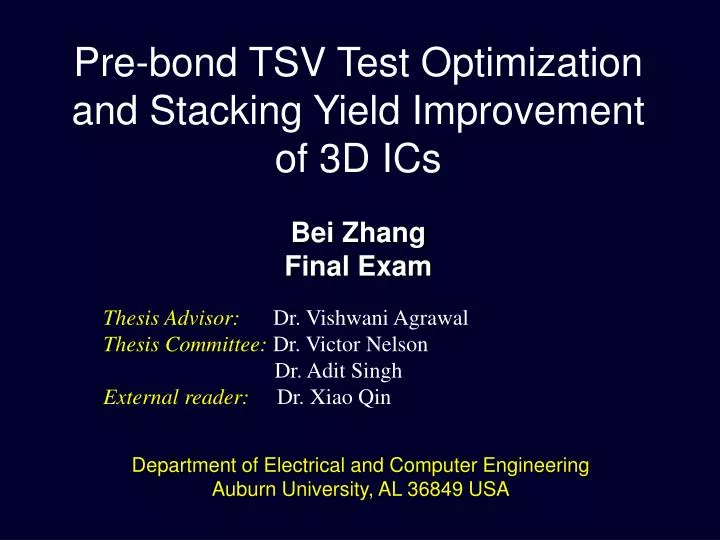
Pre-bond TSV Test Optimization and Stacking Yield Improvement of 3D ICs Bei Zhang Final Exam. Thesis Advisor: Dr . Vishwani Agrawal Thesis Committee : Dr. Victor Nelson Dr. Adit Singh External reader: Dr. Xiao Qin. Department of Electrical and Computer Engineering

E N D
Pre-bond TSV Test Optimizationand Stacking Yield Improvement of 3D ICs Bei Zhang Final Exam • Thesis Advisor:Dr. VishwaniAgrawal • Thesis Committee: Dr. Victor Nelson • Dr. Adit Singh • External reader: Dr. Xiao Qin Department of Electrical and Computer Engineering Auburn University, AL 36849 USA
ACKNOWLEGMENT • Prof. VishwaniAgrawal for his invaluable guidance throughout my work, Prof. Adit Singh and Prof. Nelsonfor being my committee members and for their courses, Prof. Xiao Qin for being my external reader, My friends and family for their support throughout my research. Bei’s final exam
Presentation Outline • Introduction • Problem Statements • Prebond TSV test optimization • Test session generation • Dynamically identify faulty TSVs • Test session scheduling • Three-step test time optimization • Wafer-on-wafer stacking yield improvement and cost reduction • Conclusion Bei’s final exam
Introduction • 3D stacked IC basic structure: • Through silicon • Via (TSV) Bei’s final exam
Introduction • RC models of defect-free pre-bond TSVs Blind TSV type 1 Blind TSV type 2 Open-sleeve TSV Bei’s final exam
Introduction • Why test TSV before bonding? • Defects arises in TSV manufacturing, such as a void within a TSV, a complete break in a TSV, a pinhole creating a leakage path between TSV and substrate, etc. • Pre-bond TSV test helps identify defective dies early in the process and avoid situations where one single bad die causes entire 3D stack to be discarded. • Pre-bond TSV test provides known good die (KGD) information for die-to-die or die-to-wafer or wafer-on-wafer fabrication process. Bei’s final exam
Introduction • RC models of defective pre-bond TSVs Resistance-defective TSV Capacitance-defective TSV Bei’s final exam
Introduction • How to test TSVs before bonding? • For Blind TSV type 1 and Open-sleeve TSV, the TSVs are buried in wafer. Test requires special per-TSV DFT circuit (e.g., BIST) to test the TSVs with only single-sided access. BIST methods have drawbacks. • For Blind TSV type 2, TSV tips are exposed. This requires special facilities to probe thinned wafers (about 50 µm thick) without damaging them. However, the relatively large pitch (40 µm) of current probing technology prohibits individual TSV probing with a realistic pitch of 10 µm. Bei’s final exam
A novel TSV probing method • Illustration of pre-bond TSV probing on the • back side of wafer.
A novel TSV probing method • Probe card configuration 1 B. Noia and K. Chakrabarty, Design-for-Test and Test Optimization Techniques for TSV-based 3D Stacked ICs. Springer, 2014.
A novel TSV probing method • Probe card configuration 2 B. Noia and K. Chakrabarty, Design-for-Test and Test Optimization Techniques for TSV-based 3D Stacked ICs. Springer, 2014.
A novel TSV probing method • Circuit model of pre-bond TSV probing Bei’s final exam
Test time of parallel TSV test • 1) Any faulty TSV within a parallel test will cause the test to fail but we cannot tell which TSV(s) is (are) faulty. • 2) On the other hand, a good parallel test implies that all TSVs within the parallel test are fault-free. S. K. Roy, S. Chatterjee, C. Giri, and H. Rahaman, “Faulty TSVs Identification and Recovery in 3D Stacked ICs During Pre-bond Testing,” in Proc. International 3D Systems Integration Conference, 2013, pp. 1–6.
Introduction • Why compound yield loss in W2W stacking? Bei’s final exam
Introduction • Wafers versus Layers in 3D W2W stacking M. Taouil, S. Hamdioui, J. Verbree, and E. Marinissen, “On Maximizing the compound yield for 3D wafer-to-wafer stacked IC," in Proc. International Test Conf., 2010, pp. 1-10. Bei’s final exam
Matching Algorithms • Matching algorithms based on Static repository: • Globally greedy matching • Iterative matching heuristic • Integer linear programming • Iterative greedy S. Reda, G. Smith, and L. Smith, “Maximizing the Functional Yield of Wafer-to-Wafer 3-D Integration,” IEEE Transactions on Very Large Scale Integration (VLSI) Systems, vol. 17, no. 9, pp. 1357–1362, Sept. 2009.
Presentation Outline • Introduction • Problem Statements • Prebond TSV test optimization • Test session generation • Dynamically identify faulty TSVs • Test session scheduling • Three-step test time optimization • Wafer-on-wafer stacking yield improvement and cost reduction • Conclusion Bei’s final exam
Problem Statement • General Problem 1 • How to quickly finish pre-bond TSV probing test. • Pinpoint each defective TSV within a reparable TSV • network (# faulty TSVs <= # redundant TSVs) as soon as possible. • 2) Identify an irreparable TSV network • (# faulty TSVs > # redundant TSVs) • as soon as possible. • General Problem 2 • How to improve the overall compound yield and • reduce the cost of wafer-on-wafer stacked 3D ICs. Bei’s final exam
Presentation Outline • Introduction • Problem Statements • Prebond TSV test optimization • Test session generation • Dynamically identify faulty TSVs • Test session scheduling • Three-step test time optimization • Wafer-on-wafer stacking yield improvement and cost reduction • Conclusion Bei’s final exam
Test Session Generation • Motivation • Compared to individual TSV test, large test time saving is possible if we test TSVs in parallel without losing the capability of identifying up to m faulty TSVs, and also guarantee the size of each test session does not exceed the resolution constraint r. Bei’s final exam
Test Session Generation • Problem statement • Given the test time t(q) for different session size q (q∈[1, r]), given the maximum number (m) of faulty TSVs within a T TSV network. Determine a series of test sessions (with size less than r) so that up to m faulty TSVs can be uniquely identified and the total test time is minimized. • Sufficient condition solving the problem • If each TSV (TSVi) is put in m + 1 sessions (say, S1, S2, · · · , Sm+1) and the intersection of any 2 out of these m + 1 sessions contains only TSVi, i.e., Si ∩ Sj = TSVifor i≠ j ∈ [1, m + 1], then up to m faulty TSVs within the network can be uniquely identified. B. Noia and K. Chakrabarty, “Identification of Defective TSVs in Pre-Bond Testing of 3D ICs,” in Proc. 20th AsianTest Symposium (ATS), 2011, pp. 187–194.
Limitations of previous heuristic method For session generation • For example, to pinpoint 1 faulty TSV in a 6-TSV network with minimum resolution constraint of r = 4, the heuristic based sessions are • {1,2,3,4}, {1,5,6}, {2,5}, {3,6}, {4}. • Careful examination shows: • Last session {4} is useless as the first 4 sessions uniquely identify any single faulty TSV. • After removing {4}, the remaining sessions are still not optimal as an optimal result is {1,2,3}, {1,4,5}, {2,4,6}, {3,5,6}, which further reduces test time by 9.7%. B. Zhang and V. D. Agrawal, “Diagnostic Tests for Pre-Bond TSV,” to appear in Proc. 26th International Conference on VLSI Design, Jan 2015..
ILP based Session Generation • Three general constraints for our ILP model (named ILP model 1): • C1. Each TSV should reside in at least m + 1 test sessions. • C2. The size of a test session ranges anywhere from 0 • (empty session) to r. • C3. Any non-empty session is supposed to be a unique • session for any TSV within it. • A unique test session for TSViis a session whose intersection with any other session containing TSViconsists of only TSVi.
Experimental results Test time comparison for a 20-TSV network Bei’s final exam
Experimental results Test time comparison for resolution constraint r = 3 Bei’s final exam
Experimental results Comparison of number of sessions for r = 4 Bei’s final exam
Presentation Outline • Introduction • Problem Statements • Prebond TSV test optimization • Test session generation • Dynamically identify faulty TSVs • Test session scheduling • Three-step test time optimization • Wafer-on-wafer stacking yield improvement and cost reduction • Conclusion Bei’s final exam
Dynamically identify faulty TSVs • Motivation • To pinpoint 1 faulty TSV in a 6-TSV network with minimum resolution constraint of r = 4. Optimal sessions are • {1,2,3}, {1,4,5}, {2,4,6}, {3,5,6} • If TSV1 is faulty, all 4 sessions need to be tested to identify it. • If TSV6is faulty, only the first 3 sessions need to be tested to • pinpoint it. • 3) Develop an algorithm to terminate the test as soon as our goal of identification is reached. Bei’s final exam
Dynamically identify faulty TSVs • Problem statement • Given a series of test sessions, how to identify up to m faulty TSVs within a T-TSV network based on these sessions with minimum identification time. • Solutions: • First, during the identification process, any “currently unnecessary” session is skipped. • Second, TSV test is terminated as soon as either all TSVs have been identified or the number of identified faulty TSV exceeds m. • B. Zhang and V. D. Agrawal, “An Optimal Probing Method of Pre-Bond TSV Fault Identification for 3D Stacked ICs,” to appear in Proc. IEEE SOI-3D-Subthreshold Microelectronics Technology Unified Conference, Oct 2014.
Experimental results Exhaustive and dynamically optimized application of TSV test sessions constructed by ILP model 1 Bei’s final exam
Presentation Outline • Introduction • Problem Statements • Prebond TSV test optimization • Test session generation • Dynamically identify faulty TSVs • Test session scheduling • Three-step test time optimization • Wafer-on-wafer stacking yield improvement and cost reduction • Conclusion Bei’s final exam
Test Session Scheduling • Motivation 1 • In real silicon, TSV yield is expected to be more than • 99% . It is most likely there is less than 1 faulty TSV within a TSV network. Probability of different number of failing TSVs within a 15-TSV network Bei’s final exam
Test Session Scheduling • Motivation 2 • In case of all TSVs within a network are fault free, all TSVs are identified as good TSVs as long as the already tested sessions covered all TSVs. Bei’s final exam
Test Session Scheduling • Problem statement • Given a series of N test sessions that can uniquely identify up to m faulty TSVs within a TSV network of T TSVs, find an optimal order to apply those sessions so that the expectation of pre-bond TSV test time is minimized for this TSV network. Test time expectation: Bei’s final exam
Test Session Scheduling • A simplified problem • Given N test sessions that can uniquely identify up to m faulty TSVs within a network of T TSVs, select M out of N sessions such that these M sessions cover each TSV at least once and the total test time of the selected M sessions is minimum. • This problem can be easily solved by constructing an ILP model (named ILP model 2). • B. Zhang and V. D. Agrawal, “An Optimized Diagnostic Procedure for Pre-Bond TSV Defects,” to appear in Proc. 32nd IEEE International Conference on Computer Design, Oct 2014. Bei’s final exam
Iterative session sorting procedure Bei’s final exam
Presentation Outline • Introduction • Problem Statements • Prebond TSV test optimization • Test session generation • Dynamically identify faulty TSVs • Test session scheduling • Three-step test time optimization • Wafer-on-wafer stacking yield improvement and cost reduction • Conclusion Bei’s final exam
Three-step Test Time Optimization • B. Zhang and V. D. Agrawal, “An Optimized Diagnostic Procedure for Pre-Bond TSV Defects,” to appear in Proc. 32nd IEEE International Conference on Computer Design, Oct 2014.
Two-step Test Time Optimization Bei’s final exam
Experimental results Expectation of number of tested sessions, defect clustering coefficient α = 1, data shows (sessions for SOS2, sessions for SOS3, reduction by SOS3) Bei’s final exam
Experimental results Expectation of test time (µs), defect clustering coefficient α = 1, data shows (test time for SOS2, test time for SOS3, reduction by SOS3) Bei’s final exam
Presentation Outline • Introduction • Problem Statements • Prebond TSV test optimization • Test session generation • Dynamically identify faulty TSVs • Test session scheduling • Three-step test time optimization • Wafer-on-wafer stacking yield improvement and cost reduction • Conclusion Bei’s final exam
Illustration of Our Efforts • A new wafer manipulation method: • B. Zhang and V. D. Agrawal, “A Novel Wafer Manipulation Method for Yield Improvement and Cost Reduction of 3D Wafer-on-Wafer Stacked ICs,” Journal of Electronic Testing: Theory and Applications, vol. 30, pp. 57–75, 2014. • B. Zhang, B. Li, and V. D. Agrawal, “Yield Analysis of a Novel Wafer Manipulation Method in 3D Stacking,” in Proc. IEEE International 3D Systems Integration Conference, 2013, pp. 1–8.
SpecificallyDesigned Wafers • Wafers fabricated with rotational symmetry: Double rotation Fourfold rotation • B. Zhang and V. D. Agrawal, “A Novel Wafer Manipulation Method for Yield Improvement and Cost Reduction of 3D Wafer-on-Wafer Stacked ICs,” Journal of Electronic Testing: Theory and Applications, vol. 30, pp. 57–75, 2014. • E. Singh, “Exploiting Rtational Symmetries for Improved Stacked Yields in W2W 3D-SICs,” in Proc. IEEE 29th VLSI Test Symposium (VTS), 2011, pp. 32–37.
Wafer Cut and Rotation • Cut rotationally symmetric wafer to sectors (subwafers): Bei’s final exam
Wafer Cut and Rotation • Sub-wafers rotation: Bei’s final exam
In case of more than 4 cuts, two methods of placement: Placement method 1 Placement method 2 Bei’s final exam
Wafer Cut and Rotation • Discussion on the number of cuts: • Illustration of Die loss on a wafer Places where no die can be placed Bei’s final exam
Relationship Between DPW and # of Cuts • # of dies per wafer: • Rule-of-thumb • In practice is 4-cuts DPW V.S. number of cuts for placement method 1 and 2