Download
1 / 2
20 likes | 167 Views
Split-gate Organic Field Effect Transistors: Control over Charge Transport Alan J. Heeger, University of California-Santa Barbara, DMR 0602280. SGFET operation: Gate1 and Gate2 voltages determine polarity of the SGFET.

E N D
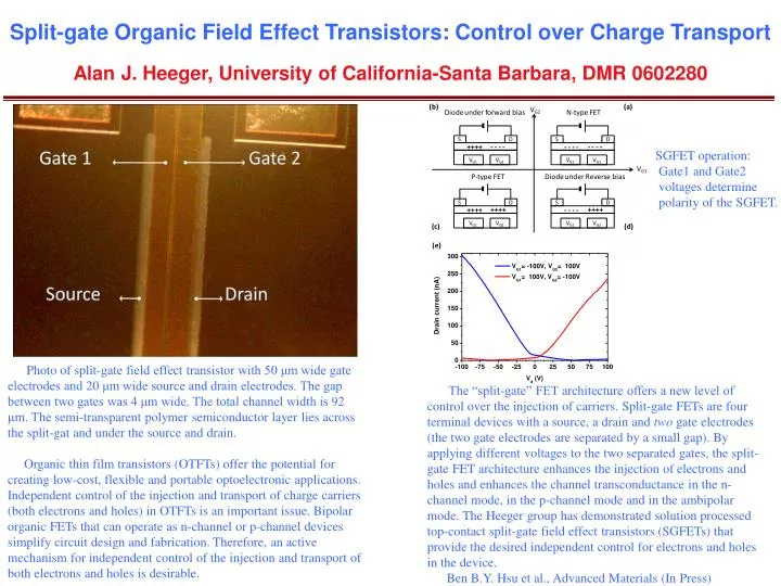
Split-gate Organic Field Effect Transistors: Control over Charge TransportAlan J. Heeger, University of California-Santa Barbara, DMR 0602280 SGFET operation: Gate1 and Gate2 voltages determine polarity of the SGFET. Photo of split-gate field effect transistor with 50 μm wide gate electrodes and 20 μm wide source and drain electrodes. The gap between two gates was 4 μm wide. The total channel width is 92 μm. The semi-transparent polymer semiconductor layer lies across the split-gat and under the source and drain. Organic thin film transistors (OTFTs) offer the potential for creating low-cost, flexible and portable optoelectronic applications. Independent control of the injection and transport of charge carriers (both electrons and holes) in OTFTs is an important issue. Bipolar organic FETs that can operate as n-channel or p-channel devices simplify circuit design and fabrication.Therefore, an active mechanism for independent control of the injection and transport of both electrons and holes is desirable. The “split-gate” FET architecture offers a new level of control over the injection of carriers. Split-gate FETs are four terminal devices with a source, a drain and two gate electrodes (the two gate electrodes are separated by a small gap). By applying different voltages to the two separated gates, the split-gate FET architecture enhances the injection of electrons and holes and enhances the channel transconductance in the n-channel mode, in the p-channel mode and in the ambipolar mode. The Heeger group has demonstrated solution processed top-contact split-gate field effect transistors (SGFETs) that provide the desired independent control for electrons and holes in the device. Ben B.Y. Hsu et al., Advanced Materials (In Press)
Split-gate Organic Field Effect Transistors: Control over Charge TransportAlan J. Heeger, University of California-Santa Barbara, DMR 0602280 • Outreach • Thin film transistors (TFTs) fabricated from semiconducting polymers continue to be of interest as components of low-cost and printable plastic electronic circuits. Integration of organic TFTs into LCD, OLED or EPD arrays leading to all-plastic displays would significantly reduce fabrication costs. • Professor Heeger has given invited (Keynote and Plenary) lectures on the results of this research at conferences in the United States, Europe and Asia. • The published manuscript shows “tunability” from ambipolar (simultaneous injection of electrons and holes) to bipolar (operating as either n-channel device or p-channel device) to unipolar operation by simply changing the gate voltages Education This is a classic interdisciplinary study involving a combination of physics, chemistry, materials science and device science. The authors include graduate students in the Materials Department (Ben B.Y. Hsu) in collaboration with post-doctoral researchers whose previous research background is in Physics (E. B. Namdas, J. D. Yuen, and S Cho). I. D.W. Samuel is a Physics Professor on sabbatical leave from St. Andrews University (Scotland).The polymer semiconductors are materials from Chemistry. The fabrication of these split-gate Field Effect Transistors required extensive use of the state-of-the-art clean room facilities at the University of California, Santa Barbara. Consequently, this split-gate device fabrication was a major step in the education of all those involved, but particularly for the graduate student (and deservedly first author) Ben B.Y. Hsu.