Download

1 / 27
270 likes | 352 Views
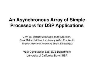
An Asynchronous Array of Simple Processors for DSP Applications. Zhiyi Yu, Michael Meeuwsen, Ryan Apperson, Omar Sattari, Michael Lai, Jeremy Webb, Eric Work, Tinoosh Mohsenin, Mandeep Singh, Bevan Baas VLSI Computation Lab, ECE Department University of California, Davis, USA. Outline.

E N D
An Asynchronous Array of Simple Processors for DSP Applications Zhiyi Yu, Michael Meeuwsen, Ryan Apperson, Omar Sattari, Michael Lai, Jeremy Webb, Eric Work, Tinoosh Mohsenin, Mandeep Singh, Bevan Baas VLSI Computation Lab, ECE Department University of California, Davis, USA
Outline • Project objectives • Key features of the AsAP processor • Design of the AsAP processor • Results
Target Applications • Computationally intensive DSP and scientific apps • Key components in many systems • Require high performance • Limited power budgets • Require innovations in architecture and circuit design
Project Objectives • Programming flexibility • High performance • Throughput • Latency • High energy efficiency • Suitable for future fabrication technologies ASIC AsAP FPGA Performance & Energy efficiency Prog. DSP Programming flexibility
Outline • Project objectives • Key features of the AsAP processor • Design of the AsAP processor • Results
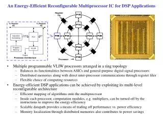
Key Features of the AsAP Processor Chip multiprocessor High performance Small memory & simple processor High energy efficiency Globally asynchronous locally synchronous (GALS) Technology scalability Nearest neighbor communication
High Performance Through Chip Multiprocessor • Increasing the clock frequency is challenging • Parallelism is more promising • Instruction level parallelism (VLIW, Superscalar) • Data level parallelism (SIMD) • Task level parallelism Deeper pipeline Higher clock frequency Increased design complexity & lower energy efficiency
Task Level Parallelism Memory Proc. Proc.2 Proc.3 Proc.1 • Well suited for DSP applications … A Task1 Task2 Task3 Task1 Task2 Task3 B A B C C Improves performance and potentially reduces memory size … … • Widely available in many DSP applications training pilots in out scram coding inter- leave mod. map loadfft inter- leave IFFT win- dow scale clip up- samp filter up- samp filter 802.11a/g wireless LAN (54 Mbps, 5 GHz) baseband transmit path
Memory Size in Modern Processors • Memory occupies much of the area in modern processors — this reduces area available for the core and consumes large amounts of power • Area and energy dissipation can be dramatically decreased with smaller memories Area breakdown other core mem TI_C64x Itanium SPARC BlGe/L [ISSCC 02, 05]
Small Memory Requirements for DSP Tasks • The memory required for common DSP tasks is quite small • Several hundred words of memory are sufficient for many DSP tasks
GALS Clocking Style • The challenge of globally synchronous systems • Design difficulty when using high clock frequencies, long clock wires caused by large chip sizes, and large circuit parameter variations • High clock power consumption and lack of flexibility to independently control clock frequencies • How about totally asynchronous design style • Lack of EDA tool support • Design complexity and circuit overhead • The GALS compromise • Synchronous blocks each operating in their own independent clock domain
Wires and On Chip Communication • Global wires are a concern • Their length doesn’t shrink with technology scaling—assuming the chip size remains the same • The ratio of global wire delay to gate delay doubles each generation • Methods to avoid global wires • Network on chip (NOC) • Local communication • Nearest neighbor communication nearest local
Outline • Project objectives • Key features of the AsAP processor • Design of the AsAP processor • Results
AsAP Block Diagram • GALS array of identical processors • Each processor is a reduced complexity programmable DSP with small memories • Each processor can receive data from any two neighbors and send data to any of its four neighbors IMem 64 words OSC FIFO 0 32 words ALU MAC Control Output FIFO 1 32 words Static config DMem 128 words Dynamic config
Single Processor Architecture • 54 32-bit instructions, among which only Bit-Reverse is algorithm specific • 9-stage pipeline IFetch Decode EXE 1 EXE 2 EXE 3 Mem. Read Src Select Result Select Write Back FIFO 0 RD Proc Output Bypass PC FIFO 1 RD Data Mem Write ALU De- code Data Mem Read Inst. Mem Multiply Accumulator A C C × + Addr. Gens. DC Mem Write DC Mem Read
Programmable Clock Oscillator • Standard cell based • Configurable frequency • Delay tunable stages using 7 parallel tri-state inverters • 5 or 9 stage selection • 1 to 128 clock divider • SR latch logic enables clean OSC halt • Results • 1.66 MHz – 702 MHz • Max gap: 0.08 MHz(1.66 – 500 MHz) Clock divider clk … … … … … ... … ... … ... … ... stage_sel reset halt
Inter-processor Communication east Read side Write side • Each processor contains two dual-clock FIFOs • Rd/Wr in separate clock domains • Gray coded Rd/Wr address across clock domains • No FIFO failures in several weeks of testing with multiple procs north SRAM west south Readlogic Writelogic east north addr addr C P U west Binary Gray & Sync. south FIFO 0 east north west FIFO 1 south Processor
Advantages of theAsAP Clocking System • Simplified clock tree design • The maximum span is < 1 mm in 0.18 µm • Scalable – easy to add processors • Improved energy efficiency • Clock halts in 9 cycles (processor dissipates leakage power only) and restores in < 1 cycle according to work availability • 53% and 65% power savings for two applications • Independent clock and voltage scaling (individual processor voltage scaling not implemented in this version)
Physical Design • 0.18 µm TSMC • Standard cell • Design flow • Completely synthesized, except oscillator • Macro memory blocks used for four main memories • Completely auto placed and routed • To simplify physical design, clock gating not implemented in this version
Chip Micrograph of the 6 x 6 Array Transistors: 1 Proc 230,000 Chip 8.5 millionMax speed: 475 MHz @ 1.8 V Area: 1 Proc 0.66 mm² Chip 32.1 mm² Power (1 Proc @ 1.8V, 475 MHz): Typical application 32 mW Typical 100% active 84 mW Worst case 144 mW Power (1 Proc @ 0.9V, 116 MHz): Typical application 2.4 mW IMem DMem 5.68 mm FIFOs OSC Single Processor 810 µm 810 µm 5.65 mm
Outline • Project objectives • Key features of the AsAP processor • Design of the AsAP processor • Results
Area Evaluation • Most of AsAP’s area is for the core (66%) • Each processor requires a very small area; more than 20x smaller than others 72 30 Processor area (mm²) 29 Area breakdown 8.3 7 20x 0.34 TI RAW Fujitsu BlGe/ AsAP C64x 4-VLIW L TI CELL/ Fujitsu RAW ARM AsAP C64x SPE 4-VLIW All scaled to 0.13 µm [ISSCC 05, 00; ISCA04; CMPON96] core mem comm
Power and Performance Power / Clock frequency / Scale * (mW/MHz) • All scaled to 0.13 µm • * Assume 2 ops/cycle for • CELL/SPE and 3.3 ops/cycle for TI C64x Note: word widths and workload not factored [ISSCC 05, 00; ISCA04; CMPON96] Higher performance ÷ area, and Lower estimated energy Peak performance density (MOPS/mm²)
JPEG Core Encoder Implementation • 9 processors • Fully functional on chip • 224 mW @ 300 MHz • ~1400 clock cycles for each 8x8 block • Similar performance and ~11x lower energy dissipation than8-way VLIW TI C62x output input Huffman Lv-shift 1-DCT DC in Huffm AC in Huffm Trans in DCT DC in Huffm AC in Huffm Quant. Zigzag Zigzag 1-DCT 8x8 DCT [MICRO 02, ISCAS 02]
802.11a/802.11g Wireless Transmitter Implementation Data bits Conv. Code Inter- leave 1 Pad Punc • 22 processors • Fully functional on chip • 407 mW @ 300 MHz 30% of 54 Mb/s • Code unscheduled and lightly optimized • ~10x performance and 35x – 75x lower energy dissipation than 8-way VLIW TI C62x Inter- leave 2 Scram Train Pilot Insert Mod. Map IFFT Mem IFFT BR IFFT Output GI/ Wind. GI/ Wind. IFFT BF IFFT Mem IFFT BF FIR FIR To D/A converter IFFT BF Output Sync IFFT Mem IFFT [SIPS 04; ICC 02]
Summary • Scalable programmable processing array • Many processors on a single chip • Reduced complexity processors with small memories • GALS clocking style • Nearest neighbor communication • Results • 0.18 µm, 475 MHz @ 1.8 V • 32 mW application power • 84 mW 100% active power • 2.4 mW application power @ 116 MHz and 0.9 V • High performance density: 475 MOPS in 0.66 mm² • Well suited for future fabrication technologies
Acknowledgments • Funding • Intel Corporation • UC Micro • NSF Grant No. 0430090 • MOSIS • UCD Faculty Research Grant • Special Thanks • R. Krishnamurthy, M. Anders, S. Mathew, S. Muroor, W. Li, C. Chen, D. Truong