Download
1 / 66
660 likes | 777 Views
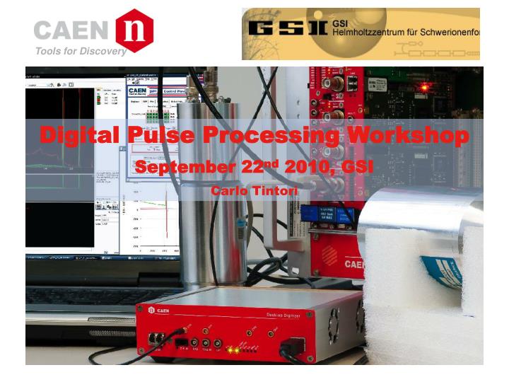
Tools for Discovery. Digital Pulse Processing Workshop September 22 nd 2010, GSI Carlo Tintori. Outline. Description of the hardware of the waveform digitizers Use of the digitizers for physics applications

E N D
Tools for Discovery Digital Pulse Processing Workshop September 22nd 2010, GSI Carlo Tintori
Outline • Description of the hardware of the waveform digitizers • Use of the digitizers for physics applications • Comparison between the traditional analog acquisition chains and the new fully digital approach • DPP algorithms: • Pulse triggering • Zero suppression • Pulse Height Analysis • Charge Integration • Gamma-Neutron discrimination • Time measurement • Multi Channel Scaler • Overview on the CAEN Digitizer family • Experimental setup description and practical demonstrations Reproduction, transfer, distribution of part or all of the contents in this document in any form without prior written permission of CAEN S.p.A. is prohibited CAEN S.p.A. reserves the right to modify its products specifications without giving any notice
Digitizers vs Oscilloscopes • The principle of operation of a waveform digitizer is the same as the digital oscilloscope: when the trigger occurs, a certain number of samples (acquisition window) is saved into one memory buffer • However, there are important differences: • no dead-time between triggers (Multi Event Memory) • multi-board synchronization for system scalability • high bandwidth data readout links • on-line data processing (FPGA or DSP) Reproduction, transfer, distribution of part or all of the contents in this document in any form without prior written permission of CAEN S.p.A. is prohibited CAEN S.p.A. reserves the right to modify its products specifications without giving any notice
Block Diagram • Mother-daughter board configuration: • The mother board defines the form-factor; it contains one FPGA for the readout interfaces and the services (power supplies, clocks, I/Os, etc…) • The daughter board defines the type of digitizer; it contains the input amplifiers, the ADCs, the FPGA for the data processing and the memories Reproduction, transfer, distribution of part or all of the contents in this document in any form without prior written permission of CAEN S.p.A. is prohibited CAEN S.p.A. reserves the right to modify its products specifications without giving any notice
Board Layout Opt. Link TRG in-out CLK in-out DAC out I/Os ADC PLL FPGA FPGA Lin. Reg. LOCAL BUS DC-DC DC-DC Memory VME Reproduction, transfer, distribution of part or all of the contents in this document in any form without prior written permission of CAEN S.p.A. is prohibited CAEN S.p.A. reserves the right to modify its products specifications without giving any notice
Multi-board synchronization (I) • Clock distribution • External Clock In/Out (differential LVDS) • Clock Distribution: • Daisy Chain: Clock-Out to Clock-In chain (the first board can act as a clock master) • Fan-Out: one clock source + 1 to N fan-out • High performance and low jitter PLL for clock synthesis • Frequency multiplication: necessary when the sampling clock frequency is high • Jitter cleaning: the PLL can reduce the jitter coming from the external clock source • Programmable clock phase adjust to compensate the cable delay Reproduction, transfer, distribution of part or all of the contents in this document in any form without prior written permission of CAEN S.p.A. is prohibited CAEN S.p.A. reserves the right to modify its products specifications without giving any notice
Multi-board synchronization (II) • Trigger and Sync Distribution • External Trigger In/Out plus 16 PIOs(*) for individual trigger propagation • Trigger Time Stamp synchronous with the ADC sampling clock • External Sync input to start-stop the acquisition synchronously and/or to keep the time stamp alignment between boards • External Trigger and Sync must be synchronous with the sampling clock, otherwise the re-synchronization causes a one clock period jitter between the boards • The trigger in-out daisy chain can be used to distribute both trigger and sync synchronously with the sampling clock • In any case, when the trigger represents also a precise time reference, it is necessary to digitize it using one channel • The trigger latency can be compensated by means of the pre-trigger size (memory look back) (*) VME boards only Reproduction, transfer, distribution of part or all of the contents in this document in any form without prior written permission of CAEN S.p.A. is prohibited CAEN S.p.A. reserves the right to modify its products specifications without giving any notice
Triggers and acquisition • Trigger types: • External Trigger (same as the ‘Ext Trigger’ in the scopes) • Software Trigger (same as the ‘Auto Trigger’ in the scopes) • Self-Trigger (same as the ‘Normal Trigger’ in the scopes) • The trigger can be common to all the channels in a board (like in the scopes) or individual • Self trigger: just a digital comparator (voltage threshold) or advanced triggers based on algorithms implemented in the FPGAs (input pulse recognition) • Programmable Acquisition Window and Pre/Post Trigger Size • Dead-Timeless Multi Event Acquisition (memory paging) • VME digitizers can use the digital I/Os to send and receive the individual self-triggers to an external logic unit (like the V1495) to make coincidences, multiplicity, neighbour trigging, etc… • Individual trigger propagation and coincidence is used for segmented germanium detectors, silicon strip detectors, wire chambers, PET, etc… Reproduction, transfer, distribution of part or all of the contents in this document in any form without prior written permission of CAEN S.p.A. is prohibited CAEN S.p.A. reserves the right to modify its products specifications without giving any notice
Fundamentals of A/D conversion • Analog Bandwidth <= Sampling rate / 2 • LSB = Dynamic Range / 2Nbit • Quantization noise: = LSB / 12 = ~ 0.3 LSB • SNR = 20 log (S/N); THD = 20 log (S/D); SINAD = 20 log (S / (N+D)) • Effective Number of bits: ENOB = (SINAD – 1.76dB) / 6.02 • Oversampling: Fovs = 4 Nadd* Fs N’bit = Nbit + NAdd • Sampling clock jitter: SNRJITTER = -20 log (2 FANALOG TJITTER) • Other sources of noise: DNL, INL Reproduction, transfer, distribution of part or all of the contents in this document in any form without prior written permission of CAEN S.p.A. is prohibited CAEN S.p.A. reserves the right to modify its products specifications without giving any notice
Digitizers for Physics Applications • Traditionally, the acquisition chains for radiation detectors are made out of mainly analog circuits; the A to D conversion is performed at the very end of the chain • Nowadays, the availability of very fast and high precision flash ADCs permits to design acquisition systems in which the A to D conversion occurs as close as possible to the detector • In theory, this is an ideal acquisition system (information lossless) • The data throughput is extremely high: it is no possible to transfer row data to the computers and make the analysis off-line! • On-line digital data processing in needed to extract only the information of interest (Zero Suppression & Digital Pulse Processing) Reproduction, transfer, distribution of part or all of the contents in this document in any form without prior written permission of CAEN S.p.A. is prohibited CAEN S.p.A. reserves the right to modify its products specifications without giving any notice
Traditional chain: example 1charge sensitive preamplifiers Reproduction, transfer, distribution of part or all of the contents in this document in any form without prior written permission of CAEN S.p.A. is prohibited CAEN S.p.A. reserves the right to modify its products specifications without giving any notice
Traditional chain: example 2trans-impedance (current sensitive) preamplifier • The QDC is not self-triggering; need a gate generator • need delay lines to compensate the delay of the gate logic Reproduction, transfer, distribution of part or all of the contents in this document in any form without prior written permission of CAEN S.p.A. is prohibited CAEN S.p.A. reserves the right to modify its products specifications without giving any notice
Benefits of the digital approach • One single board can do the job of several analog modules • Full information preserved • Reduction in size, cabling, power consumption and cost per channel • High reliability and reproducibility • Flexibility (different digital algorithms can be designed and loaded at any time into the same hardware) Reproduction, transfer, distribution of part or all of the contents in this document in any form without prior written permission of CAEN S.p.A. is prohibited CAEN S.p.A. reserves the right to modify its products specifications without giving any notice
Readout Bandwidth • Example with Mod720: • 1 sample = 12 bit = 1.5 byte • 1 channel = 1.5 byte @ 250MHz = 375 MB/s • 1 VME board = 8 channels = 3 GB/s !!! • Continuous acquisition not possible! • Example2 (triggered acquisition): • Record length = 512 samples (~ 2 s) = 768 bytes per channel • Trigger Rate = 10 KHz • 1 VME board = ~ 61 MB/s • Readout Bandwidth of CAEN digitizers: • VME with MBLT: 60 MB/s • VME with 2eSST: 150 MB/s • Optical Link: 70 MB/s • USB 2.0: 30 MB/s Reproduction, transfer, distribution of part or all of the contents in this document in any form without prior written permission of CAEN S.p.A. is prohibited CAEN S.p.A. reserves the right to modify its products specifications without giving any notice
Digital Pulse detection (self-triggering) • A good trigger is the basis for both the DPP and the Zero Suppression • The aim of the self-trigger is to identify the good pulses and trigger the acquisition on channel by channel basis • Pulse identification can be difficult because of the noise, baseline fluctuation, pile-up, fast repetition, etc… • Trigger algorithms based on a fixed voltage threshold are not suitable for most physics applications • It is necessary to apply digital filters able to reject the noise, cancel the baseline and to do shape and timing analysis Reproduction, transfer, distribution of part or all of the contents in this document in any form without prior written permission of CAEN S.p.A. is prohibited CAEN S.p.A. reserves the right to modify its products specifications without giving any notice
DPP algorithms for triggering • Timing filter RC-(CR)N: • High frequency noise rejection (RC filter mean) • Baseline restoration (CR or CR2 filter 1st or 2nd derivative) to reduce the pile-up and low frequency noise effects • Bipolar signal Zero crossing time-stamp (digital CFD) • Constraints on the Time Over Threshold and/or Zero Crossing can be added to improve the noise rejection Reproduction, transfer, distribution of part or all of the contents in this document in any form without prior written permission of CAEN S.p.A. is prohibited CAEN S.p.A. reserves the right to modify its products specifications without giving any notice
DPP for the Zero Suppression • Data reduction algorithms can be developed to reduce the data throughput: • Full event suppression: one event (acquisition window) is discarded if no pulse is detected inside the window • Zero Length Encoding: only the parts exceeding the threshold (plus a certain number of samples before and after) are saved. ZLE Reproduction, transfer, distribution of part or all of the contents in this document in any form without prior written permission of CAEN S.p.A. is prohibited CAEN S.p.A. reserves the right to modify its products specifications without giving any notice
DPP for the Pulse Height Analysis (DPP-TF) • Digital implementation of the shaping amplifier + peak sensing ADC (Multi-Channel Analyzer) • Implemented in the 14 bit, 100MSps digitizers (mod. 724) • Use of trapezoidal filters to shape the long tail exponential pulses • Pile-up rejection, Baseline restoration, ballistic deficit correction • High counting rate, very low dead time • Energy and timing information can be combined • Best suited for high resolution spectroscopy (especially Germanium detectors) Reproduction, transfer, distribution of part or all of the contents in this document in any form without prior written permission of CAEN S.p.A. is prohibited CAEN S.p.A. reserves the right to modify its products specifications without giving any notice
DPP-TF Block Diagram Reproduction, transfer, distribution of part or all of the contents in this document in any form without prior written permission of CAEN S.p.A. is prohibited CAEN S.p.A. reserves the right to modify its products specifications without giving any notice
DPP-TF / Analog Chain set-ups N1470High Voltage N968 Shaping Amplifier N957 Peak Sensing ADC Energy C.S. PRE Ge / Si DT5724 14bit @ 100MSps Digitizer + DPP-TF Energy Time Reproduction, transfer, distribution of part or all of the contents in this document in any form without prior written permission of CAEN S.p.A. is prohibited CAEN S.p.A. reserves the right to modify its products specifications without giving any notice
DPP-TF vs Analog Chain • PROs • All in one board • Stability and reproducibility • Flexibility (FPGA based algorithms) • Counting rate (low dead-time) • Ballistic deficit correction • Timing information • Wide Dynamic Range • Channel density • Synchronization and coincidences in multiple channel systems • Total Cost per Channel • CONs • Parameters set-up (need good software interface) • Getting started more difficult Energy Resolution? Better or worse depending on the conditions Reproduction, transfer, distribution of part or all of the contents in this document in any form without prior written permission of CAEN S.p.A. is prohibited CAEN S.p.A. reserves the right to modify its products specifications without giving any notice
DPP-TF: Test Results • Germanium Detectors at LNL (Legnaro - Italy) in Nov-08 and Feb-09, at GSI (Germany) on May-09, at INFN-MI on Jan-10, in Japan on Feb-10, at Duke University (USA) on Jul-10; resolution = 2.2 KeV @ 1.33 MeV (60Co) • Silicon Strip (SSSSD and DSSSD) and CsI detectors in Sweden at Lund and Uppsala (ion beam test) • NaI detectors in CAEN (see demo) • PET in U.S.A. • Homeland security application using CsI • BGO detector at ENEA ‘Centro Ricerche Casaccia’ (Rome) 60Co with Ge 228Th with DSSSD FWHM @ 1.33 MeV: 2.2 KeV Reproduction, transfer, distribution of part or all of the contents in this document in any form without prior written permission of CAEN S.p.A. is prohibited CAEN S.p.A. reserves the right to modify its products specifications without giving any notice
DPP for Segmented and Strip Detectors • Same algorithms implemented in the DPP-TF (trapezoidal filters) • Being implemented in the 14 bit, 100MSps digitizers (mod. V1724) • Neighbour channels trigger logic: it must be possible to propagate the local trigger of any channel to any other channel, either within the board or from board to board • Use of the GPIO[15:0] connected to a V1495 (general purpose programmable trigger unit) • Triggered channel save an event made of Time Stamp, Energy and a short piece of Waveform (the rising edge, typically a few tens of samples) • The memory buffers are used to pack many small events in order to increase the readout efficiency Reproduction, transfer, distribution of part or all of the contents in this document in any form without prior written permission of CAEN S.p.A. is prohibited CAEN S.p.A. reserves the right to modify its products specifications without giving any notice
Neighbour triggers: example of application • Drift of charge carriers induces a signal on adjacent electrodes • The horizontal position can be calculated as a function of the induced charges • The amplitude of the signal in the adjacent strips can be lower than the trigger threshold need neighbour triggers Reproduction, transfer, distribution of part or all of the contents in this document in any form without prior written permission of CAEN S.p.A. is prohibited CAEN S.p.A. reserves the right to modify its products specifications without giving any notice
DPP for the Charge Integration(DPP_CI) • Digital implementation of the QDC + discriminator and gate generator • Implemented in the 12 bit, high speed digitizers ( Mod. 720(*) ) • Self-gating integration; no delay line to fit the pulse within the gate • Automatic pedestal subtraction • Extremely high dynamic range • Dead-timeless acquisition (no conversion time) • Energy and timing information can be combined • Typically used for PMT or SiPM/MPPC readout and for gamma-neutron discrimination in scintillating detectors (*) Implementation in the Mod751 is being studied Reproduction, transfer, distribution of part or all of the contents in this document in any form without prior written permission of CAEN S.p.A. is prohibited CAEN S.p.A. reserves the right to modify its products specifications without giving any notice
DPP-CI Block Diagram Reproduction, transfer, distribution of part or all of the contents in this document in any form without prior written permission of CAEN S.p.A. is prohibited CAEN S.p.A. reserves the right to modify its products specifications without giving any notice
DPP-CI / Analog Chain set-ups N1470High Voltage DelayN108A QDCV792N Charge Splitter A315 CFDN842 Dual TimerN93B PMT NaI(Tl) TDC V1190 Time DT5720 12bit @ 250MSps Digitizer + DPP-CI Charge Time Reproduction, transfer, distribution of part or all of the contents in this document in any form without prior written permission of CAEN S.p.A. is prohibited CAEN S.p.A. reserves the right to modify its products specifications without giving any notice
DPP-CI vs Analog Chain • PROs • All in one board • Stability and reproducibility Flexibility • (FPGA based algorithms) • Self-Independent-Retroactive-Adaptive Gate • No conversion time (dead-timeless acquisition) • Baseline restoration • Accept positive, negative and bipolar signals • Extremely wide Dynamic Range • Coincidences between couples of channels • Total Cost per Channel • CONs • Parameters set-up (need good software interface) • Getting started more difficult • Channel density Energy Resolution? Better or worse depending on the conditions Reproduction, transfer, distribution of part or all of the contents in this document in any form without prior written permission of CAEN S.p.A. is prohibited CAEN S.p.A. reserves the right to modify its products specifications without giving any notice
DPP-CI: Test Results NaI detector and PMT directly connected to the QDC or digitizer Resolution = FWHM * 100 / Mean Reproduction, transfer, distribution of part or all of the contents in this document in any form without prior written permission of CAEN S.p.A. is prohibited CAEN S.p.A. reserves the right to modify its products specifications without giving any notice
DPP-CI: Other Tests • Tested with SiPM/MPPC detectors at Univerità dell’Insubria (Como – Italy) and in CAEN (2009/2010): • Dark Counting Rate • LED pulser • Readout of a 3x3mm Lyso Crystal + Gamma source • Readout of a scintillator tile for beta particles • 0.5 ph • 1.5 ph • 2.5 ph • Threshold scan Reproduction, transfer, distribution of part or all of the contents in this document in any form without prior written permission of CAEN S.p.A. is prohibited CAEN S.p.A. reserves the right to modify its products specifications without giving any notice
DPP for -n Discrimination • Digital implementation of the E/E or Rise Time discriminator (both are Pulse Shape Analysis) • Digital E/E: double gate charge integration (same as DPP-CI but with two gates); applied to fast output (typ. organic liquid scintillators) • Digital Rise Time discrimination: T in the Zero Crossing of two CFDs at 25% and 75%; applied to integrated output (either from C.S. preamp or digital integrator) • PSA used to discard unwanted events (typ. gammas); good events saved including waveform, energy and time stamp • Dead-timeless acquisition (no conversion time) • Algorithms tested at Duke University on July 2010 (off-line). FPGA implementation in progress. Reproduction, transfer, distribution of part or all of the contents in this document in any form without prior written permission of CAEN S.p.A. is prohibited CAEN S.p.A. reserves the right to modify its products specifications without giving any notice
-n Discrimination Block Diagram (I) Algorithms tested off-line Firmware being implemented Reproduction, transfer, distribution of part or all of the contents in this document in any form without prior written permission of CAEN S.p.A. is prohibited CAEN S.p.A. reserves the right to modify its products specifications without giving any notice
-n Discrimination Block Diagram (II) Algorithms tested off-line Firmware not planned Reproduction, transfer, distribution of part or all of the contents in this document in any form without prior written permission of CAEN S.p.A. is prohibited CAEN S.p.A. reserves the right to modify its products specifications without giving any notice
-n Discrimination: preliminary results (I) Reproduction, transfer, distribution of part or all of the contents in this document in any form without prior written permission of CAEN S.p.A. is prohibited CAEN S.p.A. reserves the right to modify its products specifications without giving any notice
-n Discrimination: preliminary results (II) Reproduction, transfer, distribution of part or all of the contents in this document in any form without prior written permission of CAEN S.p.A. is prohibited CAEN S.p.A. reserves the right to modify its products specifications without giving any notice
-n Discrimination: preliminary results (III) Reproduction, transfer, distribution of part or all of the contents in this document in any form without prior written permission of CAEN S.p.A. is prohibited CAEN S.p.A. reserves the right to modify its products specifications without giving any notice
-n Discrimination: preliminary results (IV) Reproduction, transfer, distribution of part or all of the contents in this document in any form without prior written permission of CAEN S.p.A. is prohibited CAEN S.p.A. reserves the right to modify its products specifications without giving any notice
DPP for Time Measurements • Digital implementation of the TDC + CFD • DPP-TF and DPP-CI give time stamps with the resolution of the sampling period (10 ns and 4 ns, = Ts/12); no interpolation for better timing information • Digital algorithms to implement Constant Fraction Discriminators or Timing Filters (RC-CRN) • Extremely high dynamic range • Dead-timeless acquisition (no conversion time); can manage long bursts of pulses (theoretical unlimited double pulse resolution) • Interpolation between a set of samples can increase the resolution well beyond the sampling period (up to picoseconds) • Big dependence of the resolution from the rise-time and amplitude of the pulses (V/ T) Reproduction, transfer, distribution of part or all of the contents in this document in any form without prior written permission of CAEN S.p.A. is prohibited CAEN S.p.A. reserves the right to modify its products specifications without giving any notice
Digital algorithms for Timing Analysis • Positive/negative pulses digitally transformed into bipolar pulses • The Zero Crossing doesn’t depend on the pulse amplitude • Timing filters: RCN or Digital CFD • Optional RC filter (mean filter) to reduce the HF noise • ZC interpolations: • Linear (2 points) • Cubic (4 points) • Best fit line or curve (4 or more points) Reproduction, transfer, distribution of part or all of the contents in this document in any form without prior written permission of CAEN S.p.A. is prohibited CAEN S.p.A. reserves the right to modify its products specifications without giving any notice
Digital CFD and Timing Filters NOTE: the higher ZC slope and the lower tail, the better filter Reproduction, transfer, distribution of part or all of the contents in this document in any form without prior written permission of CAEN S.p.A. is prohibited CAEN S.p.A. reserves the right to modify its products specifications without giving any notice
ZC timing errors • The timing resolution is affected by three main sources of noise: • Electronic noise in the analog signal (not considered here) • Quantization error Eq • Interpolation error Ei • Both simulations and experimental test demonstrate that there are two different regions: • When Rise Time > 5*Ts the pulse edge can be well approximated to a straight line, hence Ei is negligible. The resolution is proportional to the rise time and to the number of bits of the ADC. • When Rise Time < 5*Ts the approximation to a straight line is too rough and Ei is the dominant source of error. The resolution is still proportional to the number of bit but becomes inversely proportional to the rise time. Resolution improvement expected for cubic interpolation. • The best resolution is for Rise Time = 5*Ts, regardless the type of digitizer • The resolution is always proportional to the pulse amplitude (more precisely to the slope V/T) Reproduction, transfer, distribution of part or all of the contents in this document in any form without prior written permission of CAEN S.p.A. is prohibited CAEN S.p.A. reserves the right to modify its products specifications without giving any notice
Sampling Clock phase effect (RT<5Ts) (I) When rise time < 5*Ts, the interpolation error has a big variation with the phase between the rising edge and the sampling clock. DELAYAB = N * Ts: same clock phase for A and B same interpolation error ERRA ERRB Error cancellation in calculating TIMEAB DELAYAB = (N+0.5) * Ts: rotated clock phase for A and B different interpolation error ERRA ERRB No error cancellation. ERRA and ERRB are symmetric: twin peak distribution TIMEAB = (ZCA + ERRA) – (ZCB + ERRB) = ZCA– ZCB + (ERRA- ERRB ) Reproduction, transfer, distribution of part or all of the contents in this document in any form without prior written permission of CAEN S.p.A. is prohibited CAEN S.p.A. reserves the right to modify its products specifications without giving any notice
Sampling Clock phase effect (RT<5Ts) (II) DELAY = N * Ts DELAY = (N + 0.5) * Ts Reproduction, transfer, distribution of part or all of the contents in this document in any form without prior written permission of CAEN S.p.A. is prohibited CAEN S.p.A. reserves the right to modify its products specifications without giving any notice
Sampling Clock phase effect (RT<5Ts) (III) Vpp = 100mV Rise Time = Ts Emulation 14bit – 100MSps 12bit – 250MSps 10bit – 1GSps Reproduction, transfer, distribution of part or all of the contents in this document in any form without prior written permission of CAEN S.p.A. is prohibited CAEN S.p.A. reserves the right to modify its products specifications without giving any notice
Sampling Clock phase effect (RT<5Ts) (IV) Vpp = 100mV Mod720: 12bit 250MSps Emulation 5 ns 10 ns Rise Time 15 ns 20 ns 30 ns Reproduction, transfer, distribution of part or all of the contents in this document in any form without prior written permission of CAEN S.p.A. is prohibited CAEN S.p.A. reserves the right to modify its products specifications without giving any notice
Preliminary results: Mod724 (14 bit, 100 MS/s) DELAYAB = (N+0.5) * Ts (worst case) 50 mV StdDev (ns) 100 mV 200 mV 500 mV RiseTime (ns) Reproduction, transfer, distribution of part or all of the contents in this document in any form without prior written permission of CAEN S.p.A. is prohibited CAEN S.p.A. reserves the right to modify its products specifications without giving any notice
Preliminary results: Mod720 (12 bit, 250 MS/s) DELAYAB = (N+0.5) * Ts (worst case) 50mV 100mV 200mV StdDev (ns) 500mV RiseTime (ns) Reproduction, transfer, distribution of part or all of the contents in this document in any form without prior written permission of CAEN S.p.A. is prohibited CAEN S.p.A. reserves the right to modify its products specifications without giving any notice
Preliminary results: Mod751 (10 bit, 1 GS/s) DELAYAB = (N+0.5) * Ts (worst case) 50mV 100mV 200mV StdDev (ns) 500mV NOTE: the region with Rise Time < 5*Ts (5 ns) is missing in this plot RiseTime (ns) Reproduction, transfer, distribution of part or all of the contents in this document in any form without prior written permission of CAEN S.p.A. is prohibited CAEN S.p.A. reserves the right to modify its products specifications without giving any notice
Mod724 vs Mod720 vs Mod751 Amplitude = 100 mV 10 bit, 1 GS/s 12 bit, 250 MS/s 14 bit, 100 MS/s StdDev (ns) RiseTime (ns) Reproduction, transfer, distribution of part or all of the contents in this document in any form without prior written permission of CAEN S.p.A. is prohibited CAEN S.p.A. reserves the right to modify its products specifications without giving any notice
Mod751 @ 2 GS/s The cubic interpolation can reduce the gap between best and worst case as well as increase the resolution for small signals! StdDev (ns) RT = 1 ns - worst case RT = 5 ns RT = 1 ns - best case 2 ps ! Amplitude (mV) Reproduction, transfer, distribution of part or all of the contents in this document in any form without prior written permission of CAEN S.p.A. is prohibited CAEN S.p.A. reserves the right to modify its products specifications without giving any notice