Download
1 / 1
70 likes | 461 Views
Phase Shift Full Bridge Converter: Design Issues for a High Power and High Efficiency Application. J.M. Molina.

E N D
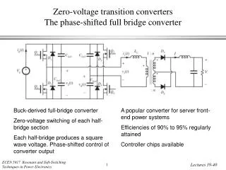
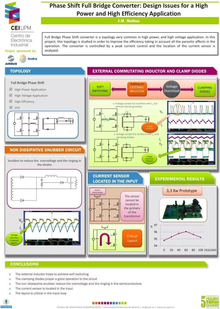
Phase Shift Full Bridge Converter: Design Issues for a High Power and High Efficiency Application J.M. Molina Full Bridge Phase Shift converter is a topology very common in high power, and high voltage application. In this project, this topology is studied in order to improve the efficiency taking in account all the parasitic effects in the operation. The converter is controlled by a peak current control and the location of the current sensor is analyzed. Project sponsoredby EXTERNAL COMMUTATING INDUCTOR AND CLAMP DIODES TOPOLOGY Full Bridge Phase Shift Adding an SOFT SWITCHING EXTERNAL INDUCTOR CLAMPING DIODES Voltage Overshoot • High Power Application • High Voltage Application • High Efficiency • Voltage across the rectifiers with Lr but without clamping diodes • ZVS Vd Cpara Llk IL VoltageOvershoot! • Voltage across the rectifiers with Lr and clamping diodes IL Vd NON DISSIPATIVE SNUBBER CIRCUIT VoltageOvershootreduced!! • Snubber to reduce the overvoltage and the ringing in the diodes CURRENT SENSOR LOCATED IN THE INPUT EXPERIMENTAL RESULTS 3,3 Kw Prototype The sensor cannot be located in the primary of the transformer SIGNAL PROCESSING Vd η IL Critical Layout VoltageOvershootreducedagain!! (%)LOAD CONCLUSIONS • The external inductor helps to achieve soft switching • The clamping diodes proper a good operation to the circuit • The non dissipative snubber reduce the overvoltage andthe ringing in the semiconductors • The current sensor is located in the input • The layout is critical in the input loop