Download
1 / 26
260 likes | 476 Views
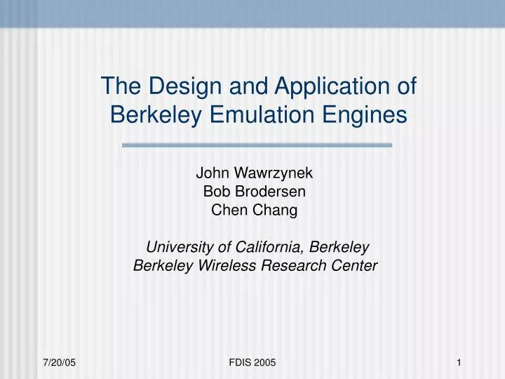
The Design and Application of Berkeley Emulation Engines. John Wawrzynek Bob Brodersen Chen Chang University of California, Berkeley Berkeley Wireless Research Center. Berkeley Emulation Engine (BEE), 2002. FPGA-based system for real-time hardware emulation:

E N D
The Design and Application of Berkeley Emulation Engines John Wawrzynek Bob Brodersen Chen Chang University of California, Berkeley Berkeley Wireless Research Center FDIS 2005
Berkeley Emulation Engine (BEE), 2002 • FPGA-based system for real-time hardware emulation: • Emulation speeds up to 60 MHz • Emulation capacity of 10 Million ASIC gate-equivalents (although not a logic gate emulator), corresponding to 600 Gops (16-bit adds) • 2400 external parallel I/Os providing 192 Gbps raw bandwidth. • 20 Xilinx VirtexE 2000 chips, 16 1MB ZBT SRAM chips. FDIS 2005
Receiver Transmitter BEE TransmitterOutputSpectrum Frame O.K. Data Match ReceiverOutput on SCSI Connector Data Out Realtime Processing Allows In-System Emulation FDIS 2005
Block Diagrams: Control Data Path User Macros S1 S2 DI DO A R/W Matlab/Simulink: Functional simulation,Hardware Emulation StateFlow, Matlab HDL CoreGen Module Compiler Black Boxes Matlab/Simulink Programming Tools:Discrete-Time-Block-Diagrams with FSMs • Tool flow developed by Mathworks, Xilinx, and UCB. • User specifies design as block diagrams (for datapaths) and finite state machines for control. • Tools automatically map to both FPGAs and ASIC implementation. • User assisted partitioning with automatic system level routing. FDIS 2005
BEE Status • Four BEE processing units built • Three in near continuous “production” use • Other supported universities • CMU, USC, Tampere, UMass, Stanford • Successful tapeout of: • 3.2M transistor pico-radio chip • 1.8M transistor LDPC decoder chip • System emulated: • QPSK radio transceiver • BCJR decoder • MPEG IDCT • On-going projects • UWB mix-signal SOC • MPEG/PRISM transcoder • Pico radio multi-node system • Infineon SIMD processor for SDR FDIS 2005
Lessons from BEE • Real-time performance vastly eases the debugging/verification/tuning process. • Simulink based tool-flow very effective FPGA programming model in DSP domain. • System emulation tasks are significant computations in their own right – high-performance emulation hardware makes for high-performance general computing. Is this the right way to build high-end (super) computers? BEE could be scaled up with latest FPGAs and by using multiple boards BEE2 (and beyond). FDIS 2005
BEE2 Hardware • Modular design scalable from a few to hundreds of FPGAs. • High memory capacity and bandwidth to support general computing applications. • High bandwidth / low-latency inter-module communication to support massive parallelism. • All off-the-shelf components no custom chips. Thanks to Xilinx for engineering assistance, FPGAs, and interaction on application development. FDIS 2005
Basic Computing Element • Single Xilinx Virtex 2 Pro 70 FPGA • 130nm technology • ~70K logic cells • 1704 package with 996 user I/O pins • 2 PowerPC405 cores • 326 dedicated multipliers (18-bit) • 5.8 Mbit on-chip SRAM • 20X 3.125-Gbit/s duplex serial communication links (MGTs) • 4 physical DDR2-400 banks • Per FPGA: up to 12.8 Gbyte/s memory bandwidth and maximum 8 GByte capacity. • Virtex 4 (90nm) out now, 2x capacity, 2x frequency. • Virtex 5 (65nm) next spring. FDIS 2005
Compute Module Diagram 10GigE or Infiniband FDIS 2005
Compute Module Completed 12/04. Module also includes I/O for administration and maintenance: • 10/100 Ethernet • HDMI / DVI • USB 14X17 inch 22 layer PCB FDIS 2005
Inter-Module Connections Global Communication Tree Stream Packets Admin, UI, NFS FDIS 2005
Alternative topology: 3D mesh or torus • The 4 compute FPGA can be used to extend to 3D mesh/torus • 6 directional links: • 4 off-board MGT links • 2 on-board LVCMOS links FDIS 2005
19” Rack Cabin Capacity • 40 compute modules in 5 chassis (8U) per rack • ~40TeraOPS, ~1.5TeraFLOPS • 150 Watt AC/DC power supply to each blade • ~6 Kwatt power consumption • Hardware cost: ~ $500K FDIS 2005
Why are these systems interesting? • Best solution in several domains: • Emulation for custom chip design • Extreme real-time signal processing tasks • Scientific and Supercomputing • Good model on how to build future chips and systems: • Massively parallel • Fine-grained reconfigurability enables: • Robust performance/power efficiency on a wide-range of problems. • Manufacturing defect tolerance. FDIS 2005
Moore’s Law in FPGA world 100X higher performance, 100X more efficient than microprocessors FPGA performance doubles every 12 months FDIS 2005
Extreme Digital-Signal-Processing BEE2 is a promising computing platform for for Allen Telescope Array (ATA) (350 antennas) and proposed Square Kilometer Array (SKA) (1K antennas) SETI spectrometer Image-formation for Radio Astronomy Research • Massive arithmetic operations per second requirement. • “Stream-based” computation model • Real-time requirement • High-bandwidth data I/O • Low numerical precision requirements • Mostly fix-point operations • Rarely needs floating point • Data-flow processing dominated • few control branch points FDIS 2005
SETI Spectrometer • Target: 0.7Hz channels over 800MHz 1 billion Channel real-time spectrometer • Result: • One BEE2 module meets target and yields 333GOPS (16-bit mults, 32-bit adds), at 150Watts (similar to desk-top computer) • >100x peak throughput of current Pentium-4 system on integer performance, & >100x better throughput per energy. FDIS 2005
FPGA versus DSP Chips • Spectrometer & polyphase filter bank (PFB): 18 mult, Correlator: 4bit mult, 32bit acc. • Cost based on street price. • Assume peak numbers for DSPs, mapped for FPGAs (automatic Simulink tools). • TI DSPs: • C6415-7E, 130nm (720MHz) • C6415T-1G, 90nm (IGHz) • FPGAs: 130nm, freq. 200-250MHz. Performance Energy Efficiency Cost-Performance Metrics include chips only (not system). FPGAs provide extra benefit at the PC board level. FDIS 2005
Active Application Areas • High-performance DSP • SETI Spectroscopy, ATA / SKA Image Formation • Scientific computation and simulation • E & M simulation for antenna design • Communication systems development Platform • Algorithms for SDR and Cognitive radio • Large wireless Ad-Hoc sensor networks • In-the-loop emulation of SOCs and Reconfigurable Architectures • Bioinformatics • BLAST (Basic Local Alignment Search Tool) biosequence alignment • System design acceleration • Full Chip Transistor-Level Circuit Simulation (Xilinx) • RAMP (Research Accelerator for MultiProcessing) FDIS 2005
Opportunity for a New Research Platform: RAMP(Research Accelerator for Multiple Processors) Krste Asanovic (MIT), Christos Kozyrakis (Stanford), Dave Patterson (UCB), Jan Rabaey (UCB), John Wawrzynek (UCB) July 2005 FDIS 2005
Change in Computer Landscape • Old Conventional Wisdom: Uniprocessor performance 2X / 1.5 yrs (“Moore’s Law”) • New Conventional Wisdom: 2X CPUs per socket / ~ 2 years • Problem: Compilers, operating systems, architectures not ready for 1000s of CPU per chip, but that’s where we’re headed • How do research on 1000 CPU systems in compilers, OS, architecture? FDIS 2005
FPGA Boards as New Research Platform • Given ~ 25 soft CPUs can fit in FPGA, what if made a 1000-CPU system from ~ 40 FPGAs? • 64-bit simple RISC at 100HMz • Research community does logic design (“gate shareware”) to create out-of-the-box Massively Parallel Processor that runs standard binaries of OS and applications • Processors, Caches, Coherency, Switches, Ethernet Interfaces, … • Recreate synergy of old VAX + BSD Unix? FDIS 2005
Why RAMP Attractive?Priorities for Research Parallel Computers 1a. Cost of purchase 1b. Cost of ownership (staff to administer it) 1c. Scalability (1000 much better than 100 CPUs) 4. Observability (measure, trace everything) 5. Reproducibility (to debug, run experiments) 6. Community synergy (share code, …) 7. Flexibility (change for different experiments) 8. Performance FDIS 2005
Why RAMP Attractive? Grading SMP vs. Cluster vs. RAMP * Costs from TPC-C Benchmark IBM eServer P5 595, IBM eServer x346/Apple Xserver, BWRC BEE2 FDIS 2005
Internet in a Box? Could RAMP radically change research in distributed computing? (Armando Fox, Ion Stoica, Scott Shenker) • Existing distributed environments (like PlanetLab) very hard to use for development: • The computers are live on the Internet and subject to all kinds of problems (security, ...) and there is no reproducibility. • You cannot reserve the whole thing for yourself and change OS or routing or .... • Very expensive to support - the reason the biggest ones are order 200 to 300 nodes, and there are lots of restrictions on using them. FDIS 2005
Internet in a Box? • RAMP promises a private "internet in a box" for $50k to $100k. • A collection of 1000 computers running independent OS that could do real checkpoints and have reproducible behavior. • We can set parameters for network delays, bandwidth, number of disks, disk latency and bandwidth, ... • Could have every board running synchronously to the same clock cycle, • so that we could do a checkpoint at clock cycle 4,000,000,000, and then reload later from that point and cause the network interrupt to occur exactly at clock cycle 4,000,000,100 for CPU 104 every single time. FDIS 2005