Download

1 / 30
570 likes | 1.07k Views
Writing a Test Bench in Verilog. Writing a Test Bench. A test bench is an HDL program used for applying stimulus to an HDL design in order to test it and observe its response during simulation.

E N D
Writing a Test Bench • A test bench is an HDL program used for applying stimulus to an HDL design in order to test it and observe its response during simulation. • In addition to the always statement, test benches use the initial statement to provide a stimulus to the circuit under test. • The always statement executes repeatedly in a loop. The initial statement executes only once starting from simulation time=0 and may continue with any operations that are delayed by a given number of units as specified by the symbol #.
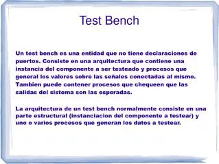
Writing a Test-Bench (2) • A stimulus module is an HDL program that has the following form. module testname Declare local reg and wire identifiers Instantiate the design module under test. Generate stimulus using initial and always statements Display the output response. endmodule • A test module typically has no inputs or outputs. • The signals that are applied as inputs to the design module for simulation are declared in the stimulus module as local reg data type. • The outputs of the design module that are displayed for testing are declared in the stimulus model as local wire data type. • The module under test is then instantiated using the local identifiers.
Writing a Test-Bench (3) The stimulus model generates inputs for the design module by declaring identifiers TA and TB as reg data type, and checks the output of the design unit with the wire identifier TC. The local identifiers are then used to instantiate the design module under test.
Writing a Test-Bench (4) • The response to the stimulus generated by the initial and always blocks will appear at the output of the simulator as timing diagrams. • It is also possible to display numerical outputs using Verilog system tasks. • $display – display one-time value of variables or strings with end-of-line return, • $write – same $display but without going to next line. • $monitor – display variables whenever a value changes during simulation run. • $time – displays simulation time • $finish – terminates the simulation • The syntax for $display,$write and $monitor is of the form Task-name (format-specification, argument list); E.g. $display(%d %b %b, C,A,B); $display(“time = %0d A = %b B=%b”,$time,A,B);
Writing a Test-Bench (5) //Dataflow description of 2-to-1-line multiplexer module mux2x1_df (A,B,select,OUT); input A,B,select; output OUT; assign OUT = select ? A : B; endmodule
Writing a Test-Bench (6) //Stimulus for mux2x1_df module testmux; reg TA,TB,TS; //inputs for mux wire Y; //output from mux mux2x1_bh mx (TA,TB,TS,Y); // instantiate mux initialbegin $monitor(”select=%b A=%b B=%b OUT=%b",TS,TA,TB,Y); TS = 1; TA = 0; TB = 1; #10 TA = 1; TB = 0; #10 TS = 0; #10 TA = 0; TB = 1; end endmodule
Test Bench for a 2 input AND Gate Design Module Truth Table
Testbench for AND Gate A Test Bench in Design Module Y
Module for AND Gate module and_2in (A, B, Out); input A, B; output Out; wire Out; assign Out = A & B; endmodule
Testbench for AND Gate `include “and_2in.v” `timescale 1ns/10ps module and_2in_tb; reg A, in; wire Y; and_2in a1( .A(A), .B(in), .Out(Y)); initial begin A=0; in=0; #20; A=0; in=1; #20; A=1; in=0; #20; A=1; in=1; #40; $stop; $finish; end endmodule
TestBench for D Flip Flop Test Bench D Q Q_n clk reset_n Design Module
TestBench for D Flip Flop in D Q clock reset TestBench Q_n clk reset_n out outbar Design Module
Module for D Flip Flop module dff (D, reset_n, clk, Q, Q_n); input D, clk, reset_n; output Q, Q_n; reg Q, Q_n; always @ (posedge clk or negedge reset_n) begin end if(reset_n == 0) begin Q <= 0; Q_n<=1; end else begin Q <= D; Q_n <= !D; end
TestBench for D Flip Flop `include “dff.v” `timescale 1ns/10ps module dff_tb; reg in, clock, reset; wire out, outbar; dff d1(.D(in), .reset_n(reset), .clk(clock), .Q(out), .Q_n(outbar));
TestBench for D Flip Flop initial begin in =0; reset =0; clock =0; #10; reset =1; #5; in=1; #10; in=0; #40; $stop; end always #10 clock = ~clock; endmodule
Counter Design • Reset the counter asynchronously through active low global reset reset_n • reset the count when the count has reached value max_count • Advance the counter through active high enable signal reset_n count[7:0] max_count[7:0] enable clk
Counter Design assign reset_count = (count == max_count); /* Generates the signal reset_count which resets the counter when the count reaches value of input max_count */ assign cnt_next = count +1; // Preincrement the value of count
Counter Design always @ (posedgeclk or negedgereset_n) begin if(reset_n ==0) count <= 8’d0; else if(reset_count == 1) count <= 8’d0; else if(enable ==1) count <= cnt_next; else count <= count; end
Counter Testbench `include “counter.v” `timescale 1ns/10ps module counter_tb; regreset_n, clk, enable; reg[7:0] max_count; wire[7:0] count; counter c1(.reset_n(reset_n), .clk(clk), .enable(enable), .max_count(max_count), .count(count) );
Counter TestBench initial begin reset_n =0; clk =0; enable =0; max_count =100; #25; reset_n =1; enable =1; #5000; $stop; end always #10 clock =~ clock; endmodule
Parallel to serial converter Design • Loads data set_data into the register when load signal is high • Shifts data when shift signal is high • Can perform both right and left shift operations • rl_n signal indicates whether to shift right or left. A high value shifts right and a low value shifts left. • data_valid is high whenever data is valid and eoc is asserted when transfer is complete
Parallel to serial converter Design reset_n data_out set_data[15:0] load data_valid shift eoc rl_n clk
Parallel to serial converter Design always @ (posedgeclk or negedgereset_n) begin if(reset_n == 0) begin data_out<=0; data_valid<=0; eoc <=0; sr <=0; cnt_reg <=0; end else if(load ==1) begin sr<= set_data; cnt_reg <=16; data_out<=0; data_valid<=0; eoc <=0; end
Parallel to serial converter Design else if ((shift==1) && (cnt_reg !=0)) begin sr <= rl_n ? (sr >> 1) : (sr <<1); data_out <= rl_n ? sr[0] : sr[15]; cnt_reg <= cnt_reg -1; data_valid <=1; eoc<=0; end
Parallel to serial converter Design else if ((shift==1) && (cnt_reg ==0)) begin sr <=sr; cnt_reg <=cnt_reg; data_out<=0; data_valid<=0; eoc <=1; end
Parallel to serial converter Design else begin sr <=sr; cnt_reg <=cnt_reg; data_out<=data_out; data_valid<=data_valid; eoc <=eoc; end
Parallel to Serial TestBench module parallel_serial_tb ; regreset_n, load, shift, rl_n, clk; reg[15:0] set_data; wire data_out, data_valid, eoc; parallel_serial p1(.reset_n(reset_n), .load(load), .shift(shift), .rl_n(rl_n), .clk(clk), . set_data(set_data), .data_out(data_out), .data_valid(data_valid), .eoc(eoc) );
Parallel to Serial TestBench initial begin reset_n =0;load=0; shift=0;rl_n=0; clk=0; set_data=0; #25; reset_n =1; set_data = 16’hAAAA; load =1; #20; load =0; shift =1; #400; shift =0; #20; rl_n =1; load=1; #20; shift=1; #500; $stop; end always #10 clk = ~clk; endmodule