Download
1 / 19
210 likes | 455 Views
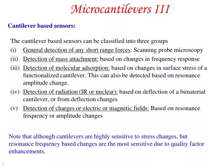
The cantilever based sensors can be classified into three groups General detection of any short range forces : Scanning probe microscopy Detection of mass attachment: based on changes in frequency response

E N D
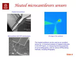
The cantilever based sensors can be classified into three groups • General detection of any short range forces: Scanning probe microscopy • Detection of mass attachment: based on changes in frequency response • Detection of molecular adsorption: based on changes in surface stress of a functionalized cantilever. This can also be detected based on resonance amplitude change. • Detection of radiation (IR or nuclear): based on deflection of a bimaterial cantilever, or from deflection changes • Detection of charges or electric or magnetic fields: Based on resonance frequency or amplitude changes Microcantilevers III Cantilever based sensors: Note that although cantilevers are highly sensitive to stress changes, but resonance frequency based changes are the most sensitive due to quality factor enhancements.
Kelvin probe technique Kelvin probe technique measures surface charge, surface potential, and surface work function. The advantages are quantitative nature, and ease of operation. Evac qVcon = qVdc = Si + Eg,Si - (semi + qs) semi Si EC Ec qs p+ Silicon Eg,Si EF,semi qVcon Ev,EF,Si Probe Tip Semiconductor Sample G. Koley and M. G. Spencer, J.Appl. Phys. 90, 337 (2001) Goutam Koley
Mathematical Model for SKPM G. Koley and M. G. Spencer, J.Appl. Phys. 90, 337 (2001) Goutam Koley
CONTROLLER SKPM Measurement System AMPLITUDE DETECTOR LASER OSCILLATOR LOCK-IN CIRCUITRY POSITION DETECTOR Vacsint Z SCANNER CONTROLLER SAMPLE Vdc Vdc MORPHOLOGY IMAGE SURFACE POTENTIAL IMAGE G. Koley and M. G. Spencer J.Appl. Phys. 90, 337 (2001) Goutam Koley
Surf. Potential Electronic characterization of dislocations 0.1 V /Div 10 nm /Div Morphology Potential G. Koley and M. G. Spencer, Appl. Phys. Lett.78, 2873 (2001) Goutam Koley
UV light Surface potential patterning using mask 20 m circle quartz mask HFET Sample (35% Al in barrier, 44 nm AlGaN layer) Goutam Koley
Spatial resolution of charge storage UV exposure through a mask of 1, 2, 5, 10 and 20 m squares Spatial resolution on the order of ~1-2 m 3.5 m G. Koley et al. JAP (2004) Goutam Koley
AFM scanning probe Measurements in GaN based transistors Biasing Probes Goutam Koley
Drain Source Surface morphology and potential profiles in dc biased transistors Gate Vd = 2V, Vg = -1.5 V Morphology Surface Potential Goutam Koley
The Cantilever effect Smaller R results in larger measurement accuracy G. Koley et al. Appl. Phys. Lett.79, 545 (2001) Goutam Koley Goutam Koley
Measurement of transients AFM scanning probe Measurement setup schematic Probe tip Drain Source Gate Gate Drain A A Source 20 resistor +ve dc bias -ve dc bias or square pulse Biasing Probes G. Koley et al. IEEE Trans. Electron Dev. 50, 886 (2003) Goutam Koley Goutam Koley
Type I: pulsed stress at Vd = 5V, Vg = pulsed from 0 to -10 V Type II: continuous stress at Vd = 20V, Vg = -12 V for 2 mins Drain current variations due to stress Vd = 1 V, Vg = 0 V during measurement. 100 m HFET 100 m HFET G. Koley et al. IEEE Trans. Electron Dev. 50, 886 (2003) Goutam Koley Goutam Koley
Drain current Surface potential Correlation between drain current and surface potential Vd = 1 V, Vg = 0 V during measurement. 100 m HFET 100 m HFET Device stressed at Vd = 20 V, Vg = -12 V for 2 mins G. Koley et al. IEEE Trans. Electron Dev. 50, 886 (2003) Goutam Koley Goutam Koley
Potential variation with distance and time 150 m HFET • Stressed at Vg = -12V, Vd = 20 V for 2 mins • Maximum variation observed ~0.3 m from the gate edge • Charges take a long time to reach equilibrium value G. Koley et al. IEEE Trans. Electron Dev. 50, 886 (2003) Goutam Koley Goutam Koley
Surface conductivity measurements (a) Morphology, (b) conductivity, and (c) overlap of the surface morphology and conductivity images Goutam Koley
Scanned gate microscopy Scanned gate microscopy is useful to determine the variation of conductivity along a thin channel, and where direct measurement of conductivity is difficult (a) Experimental set up for SGM, (c) the SGM image of a single-walled CNT bundle for Vtip = 1 V; Black corresponds to very high resistance Refer to handouts for scanning thermal microscopy Goutam Koley
Scanning capacitance microscopy Scanning capacitance technique actually measures the dC/dV signal which is inversely proportional to doping. The advantages of this technique include a large measurement range (1015 – 1020 cm-3), and resolution of <10 nm For capacitance measurement a low frequency ac voltage is applied to the sample. The ac voltage periodically changes the tip-sample capacitance. The sensor produces a high frequency signal to measure very small capacitance changes. Goutam Koley
Application of capacitance microscopy Cross-sectional measurement in a MOSFET under actual operation Goutam Koley
Applications to GaN samples • The dC/dV decreases around the dislocations indicating the reduction in the background carrier concentration Capacitance image Morphology image C-V curve Goutam Koley