Download
1 / 5
50 likes | 172 Views
Dummy and Pad C hips. Needed for various activities (interconnection tests, mass tests, assembly,…) Production of masks, processing, thinning and dicing of wafers presumably takes about 2-3 months. Dummy chips. Pad chips. 15 mm x 30 mm 50 um thick Metal pads and traces on SiO 2 /Si

E N D
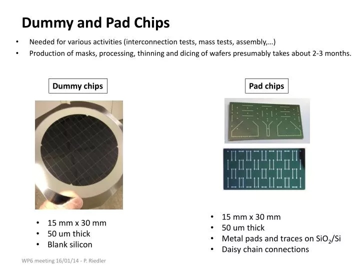
Dummy and Pad Chips • Needed for various activities (interconnection tests, mass tests, assembly,…) • Production of masks, processing, thinning and dicing of wafers presumably takes about 2-3 months. Dummy chips Pad chips • 15 mm x 30 mm • 50 um thick • Metal pads and traces on SiO2/Si • Daisy chain connections • 15 mm x 30 mm • 50 um thick • Blank silicon
Component status • Some chips left of each type, but not sufficient for the activities in 2014! • Collect needs from the different activities and start producing dummy + pad chips • WP4,6,7,8,9 Next: • Purchase wafers for dummy and pad chips • Thin and dice wafers for dummy chips • Pad chips: define layout and produce patterned wafers followed by thinning and dicing
Pad chips – main parameters tbd Chip dimension: • Approximately 15 mm x 30 mm (tbc) • Studies on stave arrangement and new beam-pipe ongoing • Study the possibility to use the full reticle length (32 mm) Number of pads: • Assume 88 contacts (32 VDDD, 32 VDDA, 8 SUB, 8 DATA, 4 CLK, 4 Conf) • Feed-back from FPC design needed (e.g. distance of pads from the edge, etc.) Pad positions: • Should be as close as possible to final layout (TDR version) • File ready soon Pad form: • Square or octagonal preferred over round pad form • Impact of the pad form on soldering needs to be evaluated on dummy chips Pad diameter: • Has to take into account the alignment precision of the holes on the FPC • Tentative diameters: 250, 300 and 350 um to be evaluated on dummy chips
Question: How many components are needed for the activities in WP6: • # of dummy chips • # of pad chips needed