Download
1 / 90
900 likes | 948 Views
Learn the fundamentals of microprocessors, machine language, and interacting with the 8085 architecture. Topics include differences between microprocessor, microcomputer, and microcontroller, instruction sets, arithmetic and logic operations, memory storage, and more.

E N D
UNIT 18085 Microprocessor R.RAJKUMAR DEPARTMENT OF CSE
Microprocessor understands Machine Language only! • Microprocessor cannot understand a program written in Assembly language • A program known as Assembler is used to convert a Assembly language program to machine language Assembly Language Program Assembler Program Machine Language Code
INTRODUCTION TO 8085 CS1007 MICROPROCESSOR AND INTERFACING Differences between: Microprocessor –silicon chip which includes ALU, register circuits & control circuits Microcomputer –a computer with a microprocessor as its CPU. Includes memory, I/O etc. Microcontroller –silicon chip which includes microprocessor, memory & I/O in a single package.
Definition of the Microprocessor • The microprocessor is a programmable device that takes in numbers, performs on them arithmetic or logical operations according to the program stored in memory and then produces other numbers as a result. CS1007 MICROPROCESSOR AND INTERFACING
1. Introduction • A microprocessor executes instructions given by the user • Instructions should be in a language known to the microprocessor • Microprocessor understands the language of 0’s and 1’s only • This language is called Machine Language
Definition (Contd.) • Lets expand each of the • Programmable device: The microprocessor can perform different sets of operations on the data it receives depending on the sequence of instructions supplied in the given program. By changing the program, the microprocessor manipulates the data in different ways. • Instructions: Each microprocessor is designed to execute a specific group of operations. This group of operations is called an instruction set. This instruction set defines what the microprocessor can and cannot do. CS1007 MICROPROCESSOR AND INTERFACING
Definition (Contd.) • Takes in: • The data that the microprocessor manipulates must come from somewhere. • It comes from what is called “input devices”. • These are devices that bring data into the system from the outside world. • These represent devices such as a keyboard, a mouse, switches, and the like. CS1007 MICROPROCESSOR AND INTERFACING
Definition (Contd.) • Numbers: • There are only 10 type of people in the world one can understand others don’t • The microprocessor has a very narrow view on life. It only understands binary numbers. • A binary digit is called a bit • The microprocessor recognizes and processes a group of bits together. This group of bits is called a “word”. • The number of bits in a Microprocessor’s word, is a measure of its “abilities”. CS1007 MICROPROCESSOR AND INTERFACING
Definition (Contd.) • Arithmetic and Logic Operations: • Every microprocessor has arithmetic operations such as add and subtract as part of its instruction set. • Most microprocessors will have operations such as multiply and divide. • Some of the newer ones will have complex operations such as square root. • In addition, microprocessors have logic operations as well. Such as AND, OR, XOR, shift left, shift right, etc. • Again, the number and types of operations define the microprocessor instruction set and depends on the specific microprocessor. CS1007 MICROPROCESSOR AND INTERFACING
Definition (Contd.) • Stored in memory : • First, what is memory? • Memory is the location where information is kept while not in current use. • Memory is a collection of storage devices. Usually, each storage device holds one bit. Also, in most kinds of memory, these storage devices are grouped into groups of 8. These 8 storage locations can only be accessed together. So, one can only read or write in terms of bytes to form memory. • Memory is usually measured by the number of bytes it can hold. It is measured in Kilos, Megas and lately Gigas. A Kilo in computer language is =1024. So, a KB (KiloByte) is 1024 bytes. Mega is 1024 Kilos and Giga is 1024 Mega. CS1007 MICROPROCESSOR AND INTERFACING
Definition (Contd.) • Stored in memory: • When a program is entered into a computer, it is stored in memory. Then as the microprocessor starts to execute the instructions, it brings the instructions from memory one at a time. • Memory is also used to hold the data. The microprocessor reads (brings in) the data from memory when it needs it and writes (stores) the results into memory when it is done. CS1007 MICROPROCESSOR AND INTERFACING
Definition (Contd.) • Produces: • For the user to see the result of the execution of the program, the results must be presented in a human readable form. • The results must be presented on an output device. • This can be the monitor, a paper from the printer, a simple LED or many other forms. CS1007 MICROPROCESSOR AND INTERFACING
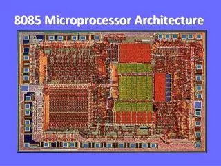
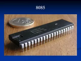
8085 Architecture • The features of INTEL 8085 are : • It is an 8 bit processor. • It is a single chip N-MOS device with 40 pins. • It has multiplexed address and data bus.(AD0-AD7). • It works on 5 Volt dc power supply. • The maximum clock frequency is 3 MHz while minimum frequency is 500kHz. • It provides 74 instructions with 5 different addressing modes. CS1007 MICROPROCESSOR AND INTERFACING
Contd.. CS1007 MICROPROCESSOR AND INTERFACING It provides 16 address lines so it can access 2^16 =64K bytes of memory. It generates 8 bit I/O address so it can access 2^8=256 input ports. It provides 5 hardware interrupts: TRAP, RST 5.5, RST 6.5, RST 7.5,INTR. It provides Acc ,one flag register ,6 general purpose registers and two special purpose registers(SP,PC). It provides serial lines SID ,SOD. So serial peripherals can be interfaced with 8085 directly.
8085 Architecture Diagram CS1007 MICROPROCESSOR AND INTERFACING
Arithmetic and Logical group CS1007 MICROPROCESSOR AND INTERFACING Accumulator: It is 8 bit general purpose register. • It is connected to ALU. • So most of the operations are done in Acc. • Temporary register: It is not available for user • All the arithmetic and logical operations are done in the temporary register but user can’t access it. • Flag: It is a group of 5 flip flops used to know status of various operations done. • The Flag Register along with Accumulator is called PSW • or Program Status Word.
Arithmetic and Logical group Contd.. CS1007 MICROPROCESSOR AND INTERFACING Flag Register is given by: S : Sign flag is set when result of an operation is negative. X : It is don’t care flip flops. Z : Zero flag is set when result of an operation is 0. Ac : Auxiliary carry flag is set when there is a carry out of lower nibble or lower four bits of the operation. CY : Carry flag is set when there is carry generated by an operation. P : Parity flag is set when result contains even number of 1’s.
Register Group CS1007 MICROPROCESSOR AND INTERFACING • Temporary registers (W,Z): These are not available for user. These are loaded only when there is an operation being performed. • General purpose: There are six general purpose registers in 8085 namely B,C,D,E,H,L.These are used for various data manipulations. • There are two special purpose registers in 8085: • SP :Stack Pointer. • PC:Program Counter.
Register Group Contd.. CS1007 MICROPROCESSOR AND INTERFACING Stack Pointer: This is a temporary storage memory 16 bit register. Since there are only 6 general purpose registers, there is a need to reuse them . • Whenever stack is to be used previous values are PUSHED on stack and then after the program is over these values are POPED back. Program Counter: It is 16 bit register used to point the location from which the next instruction is to be fetched. • When a single byte instruction is executed PC is automatically incremented by 1. • Upon reset PC contents are set to 0000H and next instruction is fetched onwards.
Instruction Register, Decoder & Control CS1007 MICROPROCESSOR AND INTERFACING • Instruction register: When an instruction is fetched , it is executed in instruction register. This register takes the Opcode value only. • Instruction decoder: It decodes the instruction from instruction register and then to control block. • Timing and control: This is the control section of µP. It accepts clock input .
Interrupt Control Serial IO Control Group • It is used to accept the serial 1 bit data by using SID and SOD signals and it can be performed by using SIM & RIM instructions. CS1007 MICROPROCESSOR AND INTERFACING • It accepts different interrupts like TRAP INT5.5,6.5,7.5and INTR.
8085 Pin Diagram CS1007 MICROPROCESSOR AND INTERFACING
8085 Pin Diagram CS1007 MICROPROCESSOR AND INTERFACING
8085 Pin Description CS1007 MICROPROCESSOR AND INTERFACING Some important pins are : • AD0-AD7: Multiplexed Address and data lines. • A8-A15: Tri-stated higher order address lines. • ALE: Address latch enable is an output signal.It goes high when operation is started by processor . • S0,S1: These are the status signals used to indicate type of operation. • RD¯: Read is active low input signal used to read data from I/O device or memory. • WR¯:Write is an active low output signal used write data on memory or an I/O device.
Contd.. CS1007 MICROPROCESSOR AND INTERFACING READY: This an output signal used to check the status of output device. If it is low, µP will WAIT until it is high. TRAP: It is an Edge triggered highest priority , non mask able interrupt. After TRAP, restart occurs and execution starts from address 0024H. RST5.5,6.5,7.5:These are maskable interrupts and have low priority than TRAP. INTR¯&INTA:INTR is a interrupt request signal after which µP generates INTA or interrupt acknowledge signal. IO/M¯:This is output pin or signal used to indicate whether 8085 is working in I/O mode(IO/M¯=1) or Memory mode(IO/M¯=0 ).
Contd.. CS1007 MICROPROCESSOR AND INTERFACING • HOLD&HLDA:HOLD is an input signal .When µP receives HOLD signal it completes current machine cycle and stops executing next instruction.In response to HOLD µP generates HLDA that is HOLD Acknowledge signal. • RESET IN¯:This is input signal.When RESET IN¯ is low µp restarts and starts executing from location 0000H. • SID: Serial input data is input pin used to accept serial 1 bit data . • X1X2 :These are clock input signals and are connected to external LC,or RC circuit.These are divide by two so if 6 MHz is connected to X1X2, the operating frequency becomes 3 MHz. • VCC&VSS:Power supply VCC=+ -5Volt& VSS=-GND reference.
Low-level/High-level languages • Machine language and Assembly language are both • Microprocessor specific (Machine dependent) so they are called • Low-level languages • Machine independent languages are called • High-level languages • For e.g. BASIC, PASCAL,C++,C,JAVA, etc. • A software called Compiler is required to convert a high-level language program to machine code
Accumulator Register Array ALU Memory Pointer Registers Flags Instruction Decoder Timing and Control Unit 2. Programming model of 8085 16-bit Address Bus 8-bit Data Bus Control Bus
8- Lines Bidirectional 16- Lines Unidirectional
Overview: 8085 Programming model • Six general-purpose Registers • Accumulator Register • Flag Register • Program Counter Register • Stack Pointer Register
Six general-purpose registers • B, C, D, E, H, L • Can be combined as register pairs to perform 16-bit operations (BC, DE, HL) • Accumulator – identified by name A • This register is a part of ALU • 8-bit data storage • Performs arithmetic and logical operations • Result of an operation is stored in accumulator
Flag Register • This is also a part of ALU • 8085 has five flags named • Zero flag (Z) • Carry flag (CY) • Sign flag (S) • Parity flag (P) • Auxiliary Carry flag (AC)
These flags are five flip-flops in flag register • Execution of an arithmetic/logic operation can set or reset these flags • Condition of flags (set or reset) can be tested through software instructions • 8085 uses these flags in decision-making process
Program Counter (PC) • A 16-bit memory pointer register • Used to sequence execution of program instructions • Stores address of a memory location • where next instruction byte is to be fetched by the 8085 • when 8085 gets busy to fetch current instruction from memory • PC is incremented by one • PC is now pointing to the address of next instruction
Stack Pointer Register • a 16-bit memory pointer register • Points to a location in Stack memory • Beginning of the stack is defined by loading a 16-bit address in stack pointer register
TIMING DIAGRAM Timing Diagram is a graphical representation. It represents the execution time taken by each instruction in a graphical format. The execution time is represented in T-states. Instruction Cycle: The time required to execute an instruction is called instruction cycle. Machine Cycle: The time required to access the memory or input/output devices is called machine cycle. T-State: The machine cycle and instruction cycle takes multiple clock periods. A portion of an operation carried out in one system clock period is called as T-state.
Timing and State Diagram CS1007 MICROPROCESSOR AND INTERFACING • The µP operates with reference to clock signal.The rise and fall of the pulse of the clock gives one clock cycle. • Each clock cycle is called a T state and a collection of several T states gives a machine cycle. • Important machine cycles are : • Op-code fetch. • Memory read. • Memory write. • I/Op-read. • I/O write.
MACHINE CYCLES OF 8085 The 8085 microprocessor has 5 basic machine cycles. • Opcode fetch cycle (4T) • Memory read cycle (3 T) • Memory write cycle (3 T) • I/O read cycle (3 T) • I/O write cycle (3 T)
Timing and State Diagram Cont.. CS1007 MICROPROCESSOR AND INTERFACING Op-code Fetch: It basically requires 4 T states from T1-T4 • S0=1,S1=1 for Op-code fetch cycle. • The ALE pin goes high at first T state always. • AD0-AD7 are used to fetch OP-code and store the lower byte of Program Counter. • A8-A15 store the higher byte of the Program Counter while IO/M¯ will be low since it is memory related operation. • RD¯ will only be low at the Op-code fetching time. • WR¯ will be at HIGH level since no write operation is done.
Timing and State Diagram Contd.. CS1007 MICROPROCESSOR AND INTERFACING Memory write Cycle: It basically requires 3T states from T1-T3 . • The ALE pin goes high at first T state always. • AD0-AD7 are used to fetch data from CPU and store the lower byte of address. • A8-A15 store the higher byte of the address while IO/M¯ will be low since it is memory related operation. • RD¯ will be HIGH since no read operation is done. • WR¯ will be at LOW level only when data fetching is done. • S0=1,S1=0 for Memory write cycle.
Memory Write Machine Cycle • The memory write machine cycle is executed by the processor to write a data byte in a memory location. • The processor takes, 3T states to execute this machine cycle.
Timing and State Diagram Contd.. CS1007 MICROPROCESSOR AND INTERFACING Memory Read Cycle: It basically requires 3T states from T1-T3 . • The ALE pin goes high at first T state always. • AD0-AD7 are used to fetch data from memory and store the lower byte of address. • A8-A15 store the higher byte of the address while IO/M¯ will be low since it is memory related operation. • RD¯ will only be low at the data fetching time. • WR¯ will be at HIGH level since no write operation is done. • S0=0,S1=1 for Memory read cycle.
I/O Write Cycle • The I/O write machine cycle is executed by the processor to write a data byte in the I/O port or to a peripheral, which is I/O, mapped in the system. • The processor takes, 3T states to execute this machine cycle
Addressing Modes of 8085 CS1007 MICROPROCESSOR AND INTERFACING To perform any operation, we have to give the corresponding instructions to the microprocessor. In each instruction, programmer has to specify 3 things: Operation to be performed. Address of source of data. Address of destination of result. The method by which the address of source of data or the address of destination of result is given in the instruction is called Addressing Modes. The term addressing mode refers to the way in which the operand of the instruction is specified.
Addressing Modes Contd.. CS1007 MICROPROCESSOR AND INTERFACING Intel 8085 uses the following addressing modes: 1. Direct Addressing Mode 2. Register Addressing Mode 3. Register Indirect Addressing Mode 4. Immediate Addressing Mode 5. Implicit Addressing Mode