Download
1 / 6
80 likes | 94 Views
If you are looking for the best PCB manufacturing machine or looking for PCB Manufacturing Toronto, or more information on Clearance and Creepage Rules for PCB Assembly, feel free to contact us.

E N D
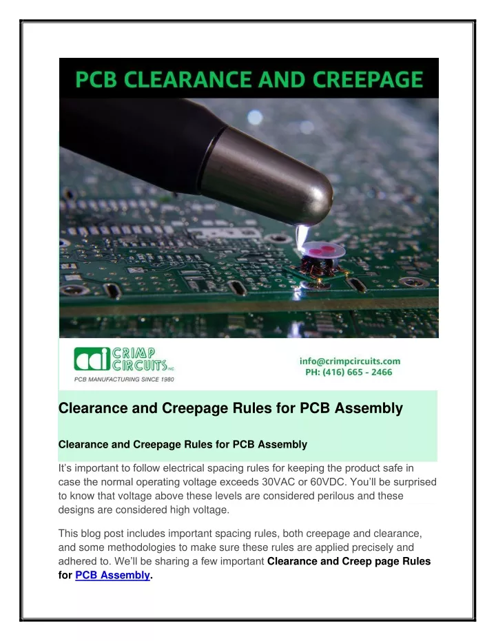
Clearance and Creepage Rules for PCB Assembly Clearance and Creepage Rules for PCB Assembly It’s important to follow electrical spacing rules for keeping the product safe in case the normal operating voltage exceeds 30VAC or 60VDC. You’ll be surprised to know that voltage above these levels are considered perilous and these designs are considered high voltage. This blog post includes important spacing rules, both creepage and clearance, and some methodologies to make sure these rules are applied precisely and adhered to. We’ll be sharing a few important Clearance and Creep page Rules for PCB Assembly.
Design Trends We aim to minimize size and maximize component density on Printed Circuit Boards and minimize the overall PCB design & assembly costs. The whole electronics product development industry is focusing on recent high-density components. This miniaturization offers some serious challenges to the designers when using mixed technology and where the design parts include the high voltage circuits. Previously, designing high voltage boards separately in a multi-board system was an easy process. But now the increased focus towards miniaturization implies that there is at least space left for multiple boards, designs employing mixed technologies have increased in the numbers. The high voltage circuits demand a new set of rules for operator’s safety. It is important to have a deep understanding of these rules and different ways to implement them while focusing on reducing the overall product size. Clearance vs. Creepage “Clearance Rules” are usually provided by the engineers in the form of spacing rules in a table or list format. In fact, the PCB design software tools indicate spacing rules as clearance rules. Though, this is not technically accurate and this becomes an significant distinction in case of high-voltage designs. The criteria for pad-to-trace, pad-to-pad, trace-to-trace spac-ing— any spacing rule implemented between conduc-tive elements over an insulating surface—is creepage, not clearance. And the spacing between two conductive elements via air is known as clearance.
The most common term ‘clearance rules' will be used to specify all spacing’s, both by design software developers and engineers. The designers need to know the actual differ-ence between clear-ance and creepage, and should ensure that they have both sets of rules when PCB design is considered high voltage. Another important thing to note is that creepage requirements are always greater or equal to the associated clearance requirements. It’s very easy to satisfy either a clearance or Creepage rule between two electrical nodes, so you need to be extra cautious during all phases of PCB design to make sure that both the rules are fulfilled.
Definitions of Clearance & Creepage: CLEARANCE: The abridged path between a conductive part and the bounding equipment’s surface, two conductive parts, or between measured through air. CREEPAGE: The abridged path between a conductive part and the bounding equipment’s surface, two conductive parts, or between measured through air, measured along the insulation’s surface. PCB CLEARANCE and CREEPAGE STANDARDS If you don’t want to learn the significance of creepage and clearance from direct experience, we’ve mentioned a few standards to help us. You need to look into IEC 60601 and IPC 2221. This standard specifies spacing between conductors as per different voltages and scenarios. There may be instances when the standards won’t guide you for solving your problem or layout your conductors. Clearance and Creep page Rules for PCB Assembly The most apparent solution to the problems associated with creepage and clearance problems is moving the conductors or components further apart. But this strategy doesn’t work with shrinking form factors and the increasing requirement of high-density PCBs. Let’s talk about a few peculiar strategies for both creepage and clearance, and evaluate other essential factors that need to be taken into account. Clearance- When looking at clearance, do not forget that it is the minimum distance in the air between nodes or conductors. You may add an insulating barrier between two different points. In case of a double-sided board, you can locate high voltage components on the low voltage components on the bottom.
There may be instances that high voltage conductors with similar voltage do not require excessive clearance from each other and also not required to be separated from low voltage conductors. Creepage- In case of creepage, you cannot simply stick things on the board’s opposite sides. Creepage is actually the distance between nodes along the insulator’s surface. Another way to maximize creepage is making a valley between the peaks. To increase the creepage, you can erase grooves or troughs into the PCB substrate. Also, you may cut slots all the way via insulator in order to maximise the distance. The same strategy is used on the power lines of high voltage insulators; those insulators have raised down their length to lengthen the creepage distance. Material- The insulating material matters a lot while dealing with creepage. When a voltage creates a conductive path along the insulator’s surface, it can break down the insulator’s surface which may result in a more conductive path between components. The characteristic which calculates this is known as the CTI (Comparative Tracking Index). Higher the material’s CTI, more insulating it is. Bounding Surface - Creepage and clearance covers your PCB’s enclosure and its conductors. While your mechanical engineer is designing enclosures. It's important to take creepage and clearance into account. Also, you can use the previously discussed strategies to handle this requirement.
If you are looking for the best PCB manufacturing machine or looking for PCB Manufacturing Toronto, you can contact us or ask for a free quote by sending us the CAD and BOM files. Want more information on Clearance and Creepage Rules for PCB Assembly, feel free to contact us. Click here: https://www.crimpcircuits.com/blog/clearance-and- creepage-rules-for-pcb-assembly/