Download

1 / 9
830 likes | 4.47k Views
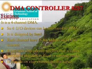
8257 DMA Controller. Block Diagram. Features. It is a 4-channel DMA. So 4 I/O devices can be interfaced to DMA It is designed by Intel Each channel have 16-bit address and 14 bit counter It provides chip priority resolver that resolves priority of channels in fixed or rotating mode.

E N D
Features • It is a 4-channel DMA. • So 4 I/O devices can be interfaced to DMA • It is designed by Intel • Each channel have 16-bit address and 14 bit counter • It provides chip priority resolver that resolves priority of channels in fixed or rotating mode. • It provide on chip channel inhibit logic. • It generates a TC signal to indicate the peripheral that the programmed number of data bytes have been transferred. • The maximum frequency is 3Mhz and minimum frequency is 250 Hz.
D0-D7: • it is a bidirectional ,tri state ,Buffered ,Multiplexed data (D0-D7)and (A8-A15). • IOR: • It is active low ,tristate ,buffered ,Bidirectional lines. • IOW: • It is active low ,tristate ,buffered ,Bidirectional control lines. • CLK: • It is the input line ,connected with TTL clock generator • RESET: • Used to clear mode set registers and status registers • A0-A3: • A0-A3 bits of memory address on the lines.
READY: • It is a asynchronous input line. • In master mode, • When ready is high it is received the signal. • HRQ: • It is used to receiving the hold request signal from the output device. • HLDA: • It is acknowledgment signal from microprocessor.
AEN (Address enable): • It is a control output line. • Used it isolate the system address ,data ,and control lines. • ADSTB: (Address Strobe) • It is a control output line. • Used to split data and address line. • TC (Terminal Count): • It is a status of output line. • It is high ,it selected the peripheral. • It is low ,it free and looking for a new peripheral. • MARK: • It is a modulo 128 MARK output line.
DRQ0-DRQ3(DMA Request): • These are the asynchronous peripheral request input signal. • The request signals is generated by external peripheral device. • DACK0-DACK3: • These are the active low DMA acknowledge output lines. • Low level indicate that ,peripheral is selected for giving the information (DMA cycle). • In master mode it is used for chip select. • Control logic block: • It contains , • Control logic • Mode set register and • Status Register.
MODE SET REGISTERS: • It is a write only registers. • It is used to set the operating modes. • This registers is programmed after initialization of DMA channel. • AL=1=Auto load mode • AL=0=Rotating mode
TCS=1=Stop after TC (Disable Channel) • TCS=0=Start after TC (Enable Channel) • EW=1=Extended write mode • EW=0=normal mode. • RP=1=Rotating priority • RP=0=Fixed priority. • EN3=1=Enable DMA CH-3 • EN3=0=Disable DMA CH-3 • EN2=1=Enable DMA CH-2 • EN2=0=Disable DMA CH-2 • EN1=1=Enable DMA CH-1 • EN1=0=Disable DMA CH-1 • EN0=1=Enable DMA CH-0 • EN0=0=Disable DMA CH-0