Download
1 / 65
660 likes | 671 Views
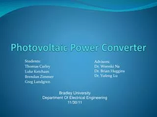
Photovoltaic Power Converter. Students: Thomas Carley Luke Ketcham Brendan Zimmer. Advisors: Dr. Woonki Na Dr. Brian Huggins. Bradley University Department Of Electrical Engineering 5/1/12. Presentation Outline. Project Summary Project Motivation Overall System Block Diagram

E N D
Photovoltaic Power Converter Students: Thomas Carley Luke Ketcham Brendan Zimmer Advisors: Dr. Woonki Na Dr. Brian Huggins Bradley University Department Of Electrical Engineering 5/1/12
Presentation Outline Project Summary Project Motivation Overall System Block Diagram Boost Converter Inverter Future Work
Project Summary Photovoltaic Array Supplies DC and AC Power Boost Converter to step up PV voltage Maximum Power Point Tracking DC-AC converter for 120Vrms 60Hz LC filter
Project Motivation • Power Electronics • Alternative Energy Sources • Useful Applications • Household grid-tie inverter • Electric drives
BP350J PV Panel • Pmax = 50W • Voltage at Pmax = 17.5V • Current at Pmax = 2.9A • Nominal Voltage = 12V • Isc = 3.2A • Voc = 21.8V
DC Subsystem Requirements • The boost converter shall accept a voltage from the photovoltaic cells. • The input voltage shall be 48 Volts. • The average output shall be 200 Volts +/- 25 Volts. • The voltage ripple shall be less than 20 Volts • The open-loop boost converter shall operate above 65% efficiency. • The boost converter shall perform maximum power point tracking. • The PWM of the boost converter shall be regulated based on current and voltage from the PV array. • The efficiency of the MPPT system shall be above 80%.
Boost Converter Test Boost Converter 20V to 66V D = .3
Key Components • MOSFET (IRFP4768PbF) • VDSS = 250V Id = 93A • Ultrafast Diode (HFA50PA60C) • VR = 600V If = 25A Trr = 50ns • Inductors (3mH) • Capacitors (6000uF)
Gate Driver IR2110
Boost Converter Simulations Output Voltage (V) 20V – 66V
Boost Converter Simulations Boost Converter Current (A) 20V-66V
Boost Converter Testing 10V to 16.5V 40% Duty Cycle Output Voltage Inductor Current
Eliminating Voltage Spikes Parasitic capacitance and inductance Diode forward recovery time Circuit Layout Add Gate Resistor to increase turn-on and turn-off time Add RC snubber
Increasing Turn off Time Turn off time increased from 92 ns to 312 ns
Reducing Voltage Spikes 20V to 66V 70% duty Without Gate Resistor And RC Snubber With Gate Resistor And RC Snubber
Boost Converter Current Efficiency = 60.7% Efficiency = 58.1% Without RC snubber and Gate Resistor With RC snubber and Gate Resistor
Future Work For Boost Converter • Optimize inductor value • Printed Circuit Board Layout • Optimize RC snubber values • Test with multiple solar panels
Maximum Power Point Tracking (MPPT) • Every PV has a V-I and P-V curve for a given insolation and temperature • The MPP is seen clearly from the P-V curve • Anytime the system is not at the MPP, it is not at it’s most efficient point I V MPP P V
Perturb and Observe (P&O) • Slight voltage perturbation • Observation of: • Change in PV power • Change in boost converter duty cycle • Make an increase or decrease in boost converter duty cycle based on observation
MPPT Algorithm Comparison • Perturb and Observe • Pros: • Very popular • Simple to implement • Con: • Power loss from perturbation • Incremental Conductance • Pro: • Tracks a rapidly changing MPP • Cons: • Increased complexity • Increased susceptibility to noise
Implementing MPPT • Spectrum Digital eZdsp F2812 • Voltage Sensing • Current Sensing • Matlab Simulink Modeling with Code Composer Studio
eZdsp F2812 features • Texas Instruments TMS320F2812 chip • 32-bit DSP Core – 150 MIPS • 18K + 64K RAM • 128K Flash • 30 MHz clock • 12 PWM outputs • 16 ADC 12 bit inputs • 60 ns conversion time
Voltage Sensing • Vpv is 0 to 24V • VADC 0 to 3.3V
Current Sensing • Ipv: 0 to 50A • Vout: 0 to 4V
Simulink Model P&O • ADC measurement • Voltage and current every 100μs • Mean value with running window of 1Hz
Simulink Model Soft Start
MPPT and Soft Start Results • Soft start duty cycle control • 0% to 30% • 5% increase every 5 seconds • Transition to MPPT after 40 seconds • MPPT duty cycle control • ADC measurements • Voltage and current every 100μs • Mean value with running window of 1Hz • 1% increase/decrease every 1 second
Power Supplies 120Vrms 60Hz input from wall 15V, 5V, and 3.3V output Consists of Transformer, Diode Rectifier, 470uF capacitor, and voltage regulators Needed for Gate Drivers, Op Amps, Sensing ICs, and other logic devices
Power Supply • Transformer (3FL20-125) • Secondary Voltage of 10VAC • Secondary Current of 0.25A RMS
AC Subsystem Goals • DC power to AC power • AC power quality
AC Subsystem Requirements • The AC side of the system shall invert the output of the boost converter. • The output of the inverter shall be AC voltage. • The output shall be 60Hz +/- 0.1Hz. • The inverter output shall be filtered by a LC filter. • The filter shall remove high switching frequency harmonics. • Total harmonic distortion of the output shall be less than 15%.
Topology - Inverter Single-phase bridge inverter
Switching Logic • Desire to control • Output frequency • Output magnitude Sinusoidal PWM!
Theory of Sinusoidal (Bipolar) PWM • The magnitude of a triangle carrier signal is compared to a sinusoidal reference • If Vreference > VcarrierPWM = high • If Vreference < VcarrierPWM = low A complementary signal drives opposite leg of H-bridge
Unipolar Sinusoidal PWM • Two sinusoids compared to a triangle reference • Each comparison drives one H-bridge leg respectively
Unipolar PWM in Action • Two comparisons • Each leg of H-bridge driven independently • 3-level output • Less harmonic distortion than bipolar PWM
Design Equations • Modulation index, mi • Frequency Modulation ratio,mf • Fundamental Output Magnitude • Output Frequency
Implications • mi can be used to control output magnitude (voltage) • Typically 0 < mi≤ 1 • Overmodulation if mi > 1 (non-linear operation) • Useful for obtaining large output power, but harmonic distortion will be large
Implications • Output Frequency • Can select mf to remove even harmonics from output spectrum • For Bipolar PWM, mf = odd integer • For Unipolar PWM, mf = even integer Example (Unipolar): fcarrier = 60 Hz ftriangle = 2520 Hz mf = 42
Output • Desire sinusoidal output • Output isn’t very sinusoidal • Use a filter • LC filter
LC Filter • Goal: Smooth inverter output to smooth AC • Second order LC filter transfer function: G(s) = 1/(L*C*s^2+1) • fcarrier < cutoff frequency < fcarrier∙ mf
Simulation • PSIM, Circuit Simulation Software • Proof of concept simulations • Bipolar PWM vs. Unipolar PWM • Effectiveness of LC filter with both schemes
PSIM Schematic (Bipolar PWM) mi = 0.8 mf = 11 Vd = 200 V