Download
1 / 41
730 likes | 1.33k Views
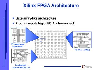
Xilinx FPGA Architecture Overview. Virtex/Spartan-II Top-level Architecture. Gate-array like architecture Configurable logic blocks Implement logic here! I/O blocks 16 signal standards Block RAM On-chip memory for higher performance Clocks & Delay-Locked Loop Interconnect resources

E N D
Virtex/Spartan-II Top-level Architecture • Gate-array like architecture • Configurable logic blocks • Implement logic here! • I/O blocks • 16 signal standards • Block RAM • On-chip memory for higher performance • Clocks & Delay-Locked Loop • Interconnect resources • Three-state internal buses
Logic Cell Capacity • A better first-order alternative to gate counting • Better comparisons among different FPGAs • Logic cell definition: • 4-input look-up table + dedicated flip-flop • Logic cells per CLB: • Xc4000/Spartan 2.375 (2 4-LUTs, 1 3-LUT, 2 FFs) • Virtex/Spartan-II 4.5 (4 4-LUTs, 1 F5MUX, 4 FFs)
Combinational Logic Function (LUT) Flip- Flop Outputs Inputs Configurable Logic Block (CLB) • Combinational logic generated in a lookup table (LUT) • Any function of available inputs • LUT output feeds CLB output or D input of flip-flop
LUT LUT LUT LUT Virtex/Spartan-II Function Generators • Four 4-input function generators • Independent inputs (4 functions of 4 inputs) • MUXF5 combines 2 LUTs to form • 4x1 multiplexer • Or any 5-input function • MUXF6 combines 2 slices to form • 8x1 multiplexer • Or any 6-input function CLB Slice MUXF6 MUXF5 Slice MUXF5
Lookup Table • Generates any function of its inputs • Typically 4 inputs • Logically equivalent to a 16 x 1 ROM InputsOutput 0000 0 0001 1 0010 1 0011 0 LUT
CLB Lookup Table Targeting LUT-based Logic • LUT limit is on inputs, not complexity • Reducing inputs/function (fan-in) to fit CLBs improves density and speed • Automatically done by Xilinx synthesis and implementation tools • Inverters are free
O1 O1 I1 N1A I1 N1 N1B N1 must go to two places, so O1 may require a second level of logic Duplicating first gate allows N1A to always be collapsed inside a single lookup table Duplicating Logic Can Improve Results • Collapsing of logic into CLBs affects number of levels required and therefore speed • The gates you use will determine mapping • Nets with a fanout >1 may be outside a CLB
AND2 Defining Lookup Tables With Gate Primitives • Example of gate primitive • Up to five inputs with all combinations of inversion • AND2B1 indicates 1 “bubbled” or inverted input • Up to nine inputs non-inverted • Add external INV primitives if desired
Stores data (D) on rising edge of clock (K) Clock enable (CE) Asynchronous clear (C) K CE C D Q X x 1 x 0 1 0 d d 0 x 0 x q D Q CE K C Flip-Flops
Additional Flip-Flop Controls • Reset (Clear) and/or Set • Global initialization (GSR) • Use to initialize all flip-flops • Programmable clock polarity • Clock enable can be left unconnected
Virtex/Spartan-II CLB Slice • 1 CLB holds 2 slices • Each slice has two sets of • Four-input LUT • Any 4-input logic function • Or 16-bit x 1 RAM • Or 16-bit shift register • Carry & Control • Fast arithmetic logic • Multiplier logic • Multiplexer logic • Storage element • Latch or flip-flop • Set and reset • True or inverted inputs • Sync. or Async. Control
Dedicated Multiplier Logic • Highly efficient ‘Shift & Add’ implementation • For a 16x16 multiplier • 30% reduction in area • 1 less logic level
On-chip RAM • All Xilinx FPGAs use RAM-based programming • Adding Write Enable to LUT creates on-chip SelectRAM memory
Data Write Enable Output Write Clock Address Data Write Enable Single-Port Output Write Clock Write Address/ Single-Port Read Address Dual-Port Output Dual-Port Read Address SelectRAM Benefits • Single-Port • Synchronous • Simple timing • Dual-Port
Memory Bandwidth and Flexibility • Virtex/Spartan-II On-Chip SelectRAM+ Memory Large FIFOs Packet Buffers Video Line Buffers Cache Tag Memory Deep/Wide SDRAM ZBTRAM SSRAM SGRAM DSP Coefficients Small FIFOs Shallow/Wide 4Kx1 2Kx2 1Kx4 512x8 256x16 16x1 Distributed RAM Block RAM External RAM bytes kilobytes megabytes 200 MHz Memory Continuum
Spartan-II Memory • CLB LUTs provide small distributed RAM (16 bits/LUT) • Block RAM provides 4K bits each • Dual read/write port. Each port has… • Independent Clock, R/W, and Enable • Independently configurable data width from 4K x 1 to 256 x 16 W R Port A Spartan-II Dual-R/WPort Block RAM Port B R W W W R R
I/O Block (IOB) • Periphery of identical I/O blocks • Input, output, or bi-directional • Direct or registered (or latched input) • Pullup/Pulldown • Programmable slew rate • Three-state output • Programmable thresholds IOB I Pad O TS Bonded to Package Pin Clocks
IPAD IBUF Use Special IOB Primitives • User explicitly defines what resources in the IOB are to be used • I/Os are defined with • 1 pad primitive • At least 1 function primitive • 1 input element, 1 output element or both • Inverters may also be pulled into IOBs
Locking Down I/O Locations • LOC=Pxx attribute defines I/O pad location(s) • Avoid locking IOBs early • Makes routing more difficult • Use IOB LOC= to lock pins late in design cycle once PCB is built • Can lock IOBs if floorplanning the connected CLBs
IPAD IBUF Use Pullups/Pulldowns • Pullup automatically connected on unused IOBs • User can specify PULLUP or PULLDOWN primitive on used IOBs • Inputs should not be left floating • Add Pullup to design inputs that may be left floating to reduce power and noise
Faster Setup With NODELAY • Delay included by default • Compensates for clock routing delay to prevent hold time • NODELAY attribute removes delay element • Creates hold time Example IOB External Data External Clock Routed Clock Pad Q D Delay X External Data Input Buffer X Delay Data External Clock Routing Delay Pad
FAST OPAD OBUF Slew Rate Control • Slew rate controls output speed • Default slow slew rate reduces noise & ground bounce • Use fast slew rate wherever speed is important • FAST parameter on output logic primitive
OBUFE OBUFT OE T OE T Output Three-State Control • Free inverter on output buffer control • Use OBUFE macro for active-high enable • Use OBUFT primitive for active-low enable
STARTUP GTS GSR Global Three-State • 3-state control either local and/or via a dedicated global net • Global three-state controlled by STARTUP... primitive
Multiple I/O Interface Standards • 16 to 20 I/O interface standards supported • CMOS, HSTL, SSTL, GTL, CTT, PCI • As many as eight banks on a device • Package dependent • Different banks can support different standards at the same time • Logic level translation • Boards with mixed standards
High Performance Routing • Hierarchical Routing • Singles, Hexes, Longs • Sparse connections on longer interconnects for high speed • Routing delay depends primarily on distance • Direction independent • Device-size independent • Predictable for early design analysis Vector Based Interconnect 2ns 2ns 2ns 2ns CLB Array
Flexible General-Purpose Interconnect • Flexible but slow if crosses many channels • Programmable switch matrix at each channel crossing • Connects across, changes direction or fans out
Switch Matrix • Bidirectional pass transistors • High routing flexibility
fn1 fn1 D Q D Q fn1 D Q Reduce Fanout • Higher fanout nets (>16 loads) are harder to route & slower • Consider duplicating source in schematic to improve routing or speed
CLB CLB CLB CLB Long Lines for High Fanout Nets • Metal lines that traverse length & width of chip • Lowest skew • Ideal for high fan-out signals • Ideal for clocking • Requires vertical or horizontal alignment of loads
Internal Three-State Buses • Two 3-state drivers per CLB • OR-AND logic implementation in place of 3-state drivers • With no drivers enabled, bus is a logic 1 • Low power • No danger of contention when multiple BUFTs enabled • No physical pullups or large capacitance to drive
General Clock Support • Use clock buffers for highest fanout clocks • Drive high-speed long line resources • Lowest skew across a device • No internal hold times • Use generic BUFG primitive • Allows software to choose best type of buffer • Allows easy migration across families • Four dedicated global low skew buffers • Dedicated input pin (clock distribution only) • Additional shared resources (i.e., long lines) • Distribute low-skew/high-fanout signals (10ns max.) • Four delay-locked loops on each device • All-digital implementation • Two global buffers associated with each DLL pair
Configuration • Schematic or HDL description is converted to a configuration file by the Xilinx development system • Configuration file is loaded into FPGA on power-up • Stored in configuration latches • Controls CLBs, IOBs, interconnect, etceteras
Configuration Bitstream • Binary programming file • Length depends only on device, not utilization • Typically 1 ms per bit (total from a few ms to <1s) • FPGA can load its configuration automatically on power-up, or under microprocessor control • Can be loaded directly into device/configuration PROM
Configuration Modes • Bit-serial configuration • Simple, uses few device pins • Controlled by FPGA (Master) or externally (Slave) • Xilinx serial proms available • Byte-parallel configuration • Can drive PROM addresses (Master) • Can be microprocessor-controlled
Configuration Pins • Configuration starts on power-up • Mode pin(s) checked to determine method • Usable as extra I/O after configuration • All I/O not used for configuration are disabled • Reconfiguration possible by pulling PROGRAM pin low
READBACK CLK DATA TRIG RIP Readback • Configuration data can be read back serially • Allows verification of programming • Readback data can include user-register values • Allows in-circuit functional verification • Requires READBACK... symbol
Boundary Scan • IEEE 1149.1-compatible boundary scan (JTAG) • Available before configuration • Configuration & readback possible via boundary scan logic
Power Consumption • CMOS SRAM technology provides low standby power • Operating power is mostly dynamic • Proportional to transition frequency of internal nodes • Xilinx segmented interconnect minimizes amount of metal capacitance to switch, minimizing power