Download
1 / 19
190 likes | 317 Views
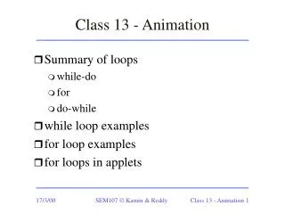
ß , dB. ß 0. -20. T (log) . 0. 1. ß. Class 13. Deriving the relative voltage transfer ratio of the CE stage using its simplyfied AC equivalent circuit Drawing the Bode plot The frequency response of ß. A v , dB. A v0. -20. 20. 40. 20. -40. 40.

E N D
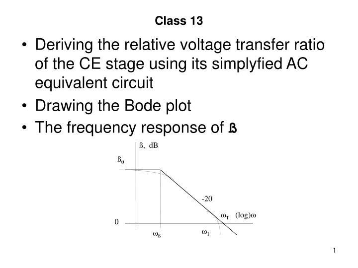
ß, dB ß0 -20 T (log) 0 1 ß Class 13 • Deriving the relative voltage transfer ratio of the CE stage using its simplyfied AC equivalent circuit • Drawing the Bode plot • The frequency response of ß
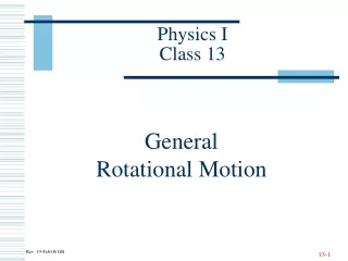
Av , dB Av0 -20 20 40 20 -40 40 c1Ec2E*≈ll in≈lh out (log) Class 13 • The resulting frequency response of a common emitter stage
Class 13 • Common emitter stage at high frequencies, if CE = 0 • in* = in(1 + g21RE) and out* out. • An improvement of the high frequency limit can only be expected if the break-point belonging to the input circuit is in dominant position (in<out), but the ‘price’ of the improvement is the decrease of the gain in a similar extent.
Class 13 • High-frequency behaviour of the common collector stage • Input circuit • The capacitance CB'C is not transformed up • The capacitance CB’E is transformed into nearly 0 capacitances • CinCC<< CinCE, that is inCC>>inCE
Class 13 • Output circuit • the output resistance of the CC stage is much smaller than that of the CE stage • 1/g21<< Rp, so outCC>>outCE • If in a chain of amplifiers CE and CC stages are present in a mixed way, the CC stages can be regarded ideal, when analyzing the high-frequency behavior of the chain.
Iout = IC Iin 2IB IC IB IB Class 13 • MTT problems from the year 2013 • 1.) Derive the relative error of the given current mirror to the left, supposing that the transistors are matched ones and B is known. • Solution: • the transistors are matched, their collector currents are equal: Iout =Iin - 2 IB • From where: h = -2/(2+B) (typically -2%)
VS+ RC ∞ 1 ∞ IN voutd RL1 ∞ 2 RB RE RL2 VS- Class 13 • 2.) Draw the connection diagram of the following circuits with no comment: • - phase splitter
Iin I Iout I IB I+IB I-IB 2IB I-IB V+ Iin Iout T3 T1 T2 R IB IB I I Class 13 • - an improved current mirror OR
iC iB C B h22 h21iB vC vB h11 E C B 1 2 E Class 13 • - a p-n-p Darlington pair of transistors • - the hybrid AC equivalent circuit of the bipolar transistor giving also the linear system of equations belonging to it • vB=h11iB+h12vC • iC=h21iB + h22vC • (where h12=0)
VS+ RC CC RL vin2 vin1 RE VS- Class 13 • - a differential amplifier with AC coupled differential input and AC coupled single ended output indicating also the inverting and non-inverting inputs
VS RC R2 R1 RE Class 13 • 3.) You are given an operating point setting circuit below:Draw its DC equivalent circuit and going the theoretical way, show how can be calculate the operation point data (IB, IC and VCE =?).
IB RB 0.6V BIB RC aVS (1+B)IB RE VS Class 13 • Solution • IB=(aVS-0.6)/(RB+[1+B]RE) • IC=BIB • VCE≈ VS-(RE+RC)IC (supposing that:IC≈IE)
VS+ RC CC2 CC1 Rg vo RL RB vin RE vg CE VS- Class 13 • 4./ Draw the connection diagram of a common emitter amplifier with bipolar transistor and a large emitter capacitance, and analyse its operation: draw its AC equivalent circuit and derive its main parameters: Av, Rin and Rout.
Rgii B C io vg vi RB vB g11 g21vB g22 RC vo RL E Rp = RC x RL x () Class 13 • The AC equivalent circuit • The voltage gain: Av=-g21vBRp/vB=-g21Rp • The input resistance: Rin=RBx(1/g11) • The output resistance: Rout=RCx(1/g22)≈RC
VS+ RC RC RL vin2 vin1 vod RB RB RE VS- Class 13 • 5.) Draw the connection diagram of a basic differential amplifier with bipolar transistors, and analyse its operation with pure common mode input voltages, deriving the parameters(g22=0): Avcc, Avdc and Rinc.
voc RC vinc RB 2RE Class 13 • The AC equivalent • Avcc=-g21RC/(1+g212RE) • Avdc=0 • Rinc=0.5(RBx[h11+h212RE)
Class 13 • 6.) The input voltages of a DC coupled differential input differential output two-transistor amplifier are: • vi1 = 4.025 V and vi2 = 3.975 V. The following data of the amplifier are known: • Avdd = 100; Avcd = 0; D = 103; CMRR = 104. Calculate the value of the differential mode and common mode components of the output voltages (vod , voc = ?).
Class 13 • Solution • The differential and common mode components of the input voltages: • vid=vi1-vi2=4.025-3.975=0.05 V • vic=0.5(vi1+vi2)=0.5(4.025+3.975)=4.00 V • From the definitions of the D and CMRR Avcc=0.1; Avdc=0.01 • The calculation of the output voltage’s components: vod=…=5.04V; voc=…=0.4V
Class 13 • On Class 14 (March 13, 8.15 am., room QBF08): • 1st Mid-Term-Test