Download
1 / 12
130 likes | 255 Views
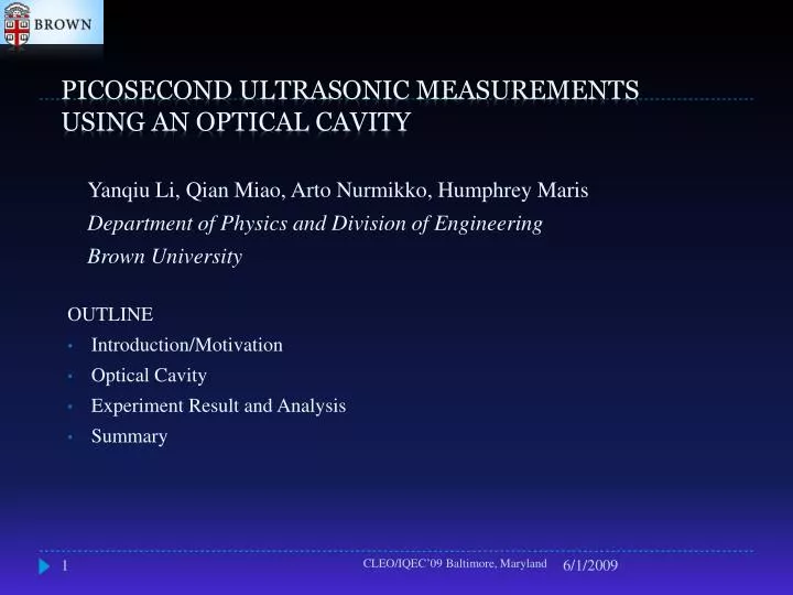
PICOSECOND ULTRASONIC MEASUREMENTS USING AN OPTICAL CAVITY. Yanqiu Li, Qian Miao, Arto Nurmikko , Humphrey Maris Department of Physics and Division of Engineering Brown University. OUTLINE Introduction/Motivation Optical Cavity Experiment Result and Analysis Summary. 0. 100. 200.

E N D
PICOSECOND ULTRASONIC MEASUREMENTS USING AN OPTICAL CAVITY Yanqiu Li, Qian Miao, ArtoNurmikko, Humphrey Maris Department of Physics and Division of Engineering Brown University OUTLINE • Introduction/Motivation • Optical Cavity • Experiment Result and Analysis • Summary CLEO/IQEC’09 Baltimore, Maryland
0 100 200 300 Introduction/Motivation – PicosecondUltrasonics 4x10⁻⁵ • Picosecond ultrasonics has become a standard technique for non-destructive ultrasonic investigation of features of thin films and nanostructures, such as film thickness, internal cracks, etc. • Plays important role in wafer inspection in the semiconductor industry. • Two significant challenges include small strain and piezo-optic effect. Pump light pulse sends out strain pulse, that induces change in the optical properties of the film (piezo-optic effect). Film (d~200nm) Substrate Piezo-optical coefficients Returning strain pulse 2x10⁻⁵ Time delayed Probe light pulses. Detect returning of the strain pulse by monitor the change in the reflectivity of the probe. 2nd round trip of the strain pulse 1st round trip of the strain pulse Launching of the longitudinal strain pulse Result of measurement of DR/R of an Aluminum film • SMALL • even zero, e.g. at l=800nm, of Cu (key material for interconnect wiring in the semiconductor industry). • SMALL • e.g. for Cu, with 10mW absorbed laser power, focal spot size of 20 mm • hmax ~10-5 z=0 z=d PROBE TIME DELAY (ps) CLEO/IQEC’09 Baltimore, Maryland
30 1 Need to maximize cavity Q factor 15 The Optical Cavity 20 z=-w 0.7 10 0.8 DBR Film (d~200nm) Substrate 0.4 10 Probe, k0 5 0.6 q 0 0 0.4 Only exists in the cavity case Sample Rs =|rs|2=0.85, varying RR , plotting Enhancement factors -5 -10 0.1 0.95 0.8 0.2 0.1 R 0.8 0.7 0.4 0.95 0.4 0.7 -10 -20 0 0 p -p a -p/4 0.85 0 z=0 z=d 0.1 -15 0 a -p/4 p/4 0.8 0.95 a CLEO/IQEC’09 Baltimore, Maryland
Probe Incidence angle 0o Pump Incidence angle 4o Maximizing the Enhancement Factors 1.0 1.0 Choose RR (0.84 at 800nm) close to RS Minimize spread in l, q, and w Decrease the spread in wavelength using a laser line filter Decrease the spread in the incidence angle of the probe beam Spectrum of Laser Light • Convert spread in the angle to the spread in the wavelength, by considering kz= 2pcosq/l0Dl=l0tanqDq 0.8 Dl= 12.5 nm 0.8 Laser line filter Dl= 3.2 nm 0.6 Measured Reflectivity of Al film (RAl=0.793) with cavity • For example l0=800nm • q=p/4, Dq=0.1, Dl = 80 nm • q=0, Dq=0.1, Dl = 1 nm • Probe needs to be at normal incidence 0.6 Measured Reflectivity of Cu film (RCu=0.955) with cavity 0.4 Cavity R Rpump Rprobe 0.2 Dl= 12.5 nm 0.4 Decrease the spread in the spacing of the cavity 2005 • The angle between the two reflecting surfaces of the cavity needs to be less than 10-4 rad 1500 1600 1700 1900 2000 2100 1800 0.0 Dl= 3.2 nm CAVITY SPACING(nm) 1900 1950 2000 2100 2050 Shifts pump resonance (maximum energy absorption) 5nm away from probe resonance to 2005nm, where DRprobe is largest. CAVITY SPACING (nm) CLEO/IQEC’09 Baltimore, Maryland
0 100 200 300 Result of Al film (190 nm) with/wo cavity (a) Al film 1.0 • Enhancement factor with the use of the cavity is bigger than 170. 4x10⁻⁵ 0.8 2x10⁻⁵ 0.6 (b) Same Al film with cavity -0.5x10⁻³ 0.4 Rpump -1x10⁻³ Rprobe 0.2 Measured at w=2005nm 2005 -1.5x10⁻³ 0.0 CAVITY SPACING(nm) 1900 1950 2000 2100 2050 PROBE TIME DELAY (ps) CLEO/IQEC’09 Baltimore, Maryland
In the vicinity of the 5th Resonance Mode Measured values of DR(t)/R for Aluminum film at 9 cavity spacing in the vicinity of the 5th resonance mode. 6x10⁻⁴ 2x10⁻⁴ 3 4x10⁻⁴ 2 0 4 1 2x10⁻⁴ -2x10⁻⁴ 9 5 8 0 6 Calculated |DR/R| 7 Measured DR/R values -4x10⁻⁴ 1980 1990 2000 2010 2020 CAVITY SPACING (nm) 50 100 PROBE TIME DELAY (ps) CLEO/IQEC’09 Baltimore, Maryland
3x10⁻⁶ 0 1.5x10⁻⁶ -2x10⁻⁴ 0.0 -4x10⁻⁴ -1.5x10⁻⁶ -200 -100 0 100 200 Data Fitting 6x10⁻⁶ 1st echo of Al film 3x10⁻⁶ Measured result Result of best fit Deduced strain pulse DR/R 0 h PROBE TIME DELAY (ps) 1st echo of Al film with cavity at w = 2005nm -3x10⁻⁶ z (nm) DR/R Compare with the theoretical model When z>0 When z<0 (Thomsen et al ,1986) Result of best fit Measured result -6x10⁻⁶ We can also determine the piezo-optical coefficients of the film 30 -30 -20 -10 0 10 20 20 30 10 0 -10 -30 -20 PROBE TIME DELAY (ps) CLEO/IQEC’09 Baltimore, Maryland
0 -2x10⁻⁴ -4x10⁻⁴ Two contributions to Da DR/R Surface displacement of the film DR/R Piezo-optical effect Piezo-optic effect Surface displacement Surface displacement of the film Dw on the order of 10-3 nm can be detected high sensitivity with the use of the cavity Measured result at w=2005nm -30 30 -10 0 -20 10 20 PROBE TIME DELAY (ps) CLEO/IQEC’09 Baltimore, Maryland
Cu Thin Film (180nm) • Cu is the KEY material for interconnect wiring in the semiconductor industry. • It is important and interesting to improve picosecond ultrasonic measurements of Cu at 800nm. • At l=800nm (wavelength of the laser used in the present experiment, also the most common wavelength of commercial compact ultrafast lasers), the piezo-optic coefficients of Cu are zero (Gerhardt, 1968). • When the cavity is not used, the only contribution to DR/R comes from the piezo-optic effect of the film. • NO acoustic signals can be see DR/R 6x10⁻⁷ • 4x10⁻⁷ • 2x10⁻⁷ 0 0 20 40 60 • PROBE TIME DELAY (10-12 Sec) CLEO/IQEC’09 Baltimore, Maryland
Cu Thin Film (180nm) With Cavity • For Cu at l=800nm, D|rS|=0,DfS=0, because piezo-optical coefficients are zero. • Only contribution to DR(t)/R from surface displacement Dw • Theoretical model where h1 is the returning strain pulse using theoretical (Thomsen) model, z ’ the diffusion length. • Measured result smaller and broader due to attenuation or approximation for the initial stress 2x10⁻⁴ Calculated result using z’=100nm Calculated result using z’=150nm DR/R 1x10⁻⁴ Measured result at w = 1606nm background removed 0 0 50 150 100 200 250 PROBE TIME DELAY (ps) CLEO/IQEC’09 Baltimore, Maryland
Summary • Significant signal enhancement, bigger than 170 for Al film • Able to perform measurements on materials with small piezo-optical coefficients, Cu, key material in semiconductor industry • Able to determine the actual shape of the returning acoustic pulse enriching the total amount of information in the picosecond ultrasonic measurements • Sensitive to very small displacement ~10-3 nm • The technique can be used for a wide variety of ultrafast optical pump-and-probe experiments. Acknowledgement • Zygo Corporation for Grant Support • Fan Yang, Tom Grimsley for helpful discussions CLEO/IQEC’09 Baltimore, Maryland
Measurement of the Effective Cavity Spacing 2.8 mm 3.2 mm 3.0 mm CLEO/IQEC’09 Baltimore, Maryland