Download
1 / 20
200 likes | 302 Views
ELECTROMECHANICAL RESPONSE OF SLIDING CDWs: VOLTAGE-INDUCED TORSIONAL STRAIN IN TaS 3. Hao Zhang, John Nichols, C. Sandumali Weerasooriya, and Joseph Brill University of Kentucky Thanks to Vadim Pokrovskii and Damir Dominko for helpful discussions and Robert Thorne for samples. Outline

E N D
ELECTROMECHANICAL RESPONSE OF SLIDING CDWs: VOLTAGE-INDUCED TORSIONAL STRAIN IN TaS3 Hao Zhang, John Nichols, C. Sandumali Weerasooriya, and Joseph Brill University of Kentucky Thanks to Vadim Pokrovskii and Damir Dominko for helpful discussions and Robert Thorne for samples.
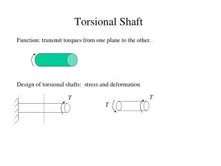
Outline • Review of previous electromechanical effects in orthorhombic TaS3* • Our experiments on voltage-induced torsional strain (VITS) in TaS3 • Our model • Problem: Time constants * Orthorhombic TaS3: the “fruit fly” of electromechanical effects in CDW materials: • Large effects • Crystal sizes (typically (1mm-1cm) x 10 mm x 1 mm) make them “easy” to deform (bend, twist) crystal.
Shear compliance, J = 1/G In 1984, it was discovered (using vibrating reed measurements) that the Young’s modulus decreased by ~ 2% with CDW depinning. In 1987, it was discovered (torsional oscillator measurements) that the shear modulus (G) decreases by ~ 20%. In both cases, the “internal friction” = tan d[damping, e.g. tan d = Im(J)/Re(J)] also increased when the CDW was depinned. Zhan and Brill (1997)
e.g. Simple (Debye) Relaxation: (M(w,V)/M0)-1 = 1 + A/(1 + iwt) Mozurkewich (1990): Voltage dependence of elastic moduli is due to strain dependence of kF changing the configuration of CDW phase domains, which change with relaxation time t(V). Relaxation strengths Young’s: AY = (YCDW/Y0) (1+ ∂lnkF/∂ε//)2 Shear: AG = (YCDW/G0) (∂lnkF/∂εf)2 For V<VT, t = ∞, so the CDW spring is locked in place. Zhan and Brill (1997)
1991: Hoen, et al, found that the length of TaS3 crystal changes as you depin the CDW, with DL/L ~ 10-6. • Changes are hysteretic, occur near threshold, and then saturate for large voltages (unlike changes in modulus). • Model: Electric field near threshold strains the CDW, which couples to strain of the lattice.
The CDW compresses at the positive contact and stretches at the negative contact. Most of this change is hysteretic, due to pinning of the CDW phase for voltages below threshold. (VT – Von is the “phase-slip voltage”.) phase Itkis, et al (1986) The changes in q put longitudinal stress on the lattice, with longitudinal “trans-modulus” m// ~ 6YCDW ~ 40 GPa. [Golovnya et al (2002)]. (The total length changes are small because the changes in q at the two ends are only slightly different.)
By applying square waves to the sample, we measured how quickly the CDW q can cross the hysteresis loop. The change in q is relaxational: near Von, t0 < 10 ms and is determined by diffusion of the CDW phase. [t0(Von) = L2/p2D, where D is proportional to the square of the phason velocity -- (ECRYS-2008 proceedings).] At higher voltages, relaxation is enhanced (t0 falls) due to CDW phase-slip (i.e. current). Rai and Brill, (2004)
Pokrovskii, et al, (2007) found that crystals of TaS3 also twist under applied dc voltage. The observed twist: • occurs in the CDW state • has onset for V ~ VT and doesn’t go away if V → 0, but reverses if V ~ -VT (i.e. has hysteresis similar to length and CDW deformations • is “sluggish”: if the CDW is depinned with ac current, torsion disappears at high frequencies. (There is also a smaller, faster and non-hysteretic voltage induced strain.) • Since TaS3 is orthorhombic and CDW is “linear”, not clear what could give rise to “voltage-induced torsional strain” (VITS) . • (How does it know which way to turn?)
Our Measurements Magnetic Wire (Transducer) Gold film on half the sample so E=0, pinning the CDW on this side. B sample Triangle-wave or square-wave voltages applied to sample ~ 2 mm Sample inside RF (430 MHz, Q=300) cavity; when sample twists, it changes resonant frequency. Application of dc B allows us to apply external torque. Application of ac B allows us measure V-dependence of shear compliance (J) and VT and to approximately calibrate the cavity response. Measure cavity frequency shifts ( twist angle) as functions of time or frequency of applied voltage.
Sample C, T = 78 K • Hysteresis loops very sluggish (take > 10 sec to develop) (Torsional resonant frequency ~ 530 Hz). • Hysteresis loops are not symmetric functions of V (both shape and dynamics different for two polarities). • Von (↑↓), where twist starts changing, is typically below VT (where compliance starts changing). Applying dc voltage to sample and small sinusoidal ac to magnet. Applying triangle wave (period T) to sample. -Von
Sample C, T = 78 K The onset voltage for the VITS is more easily seen by applying symmetric square waves (frequency w/2p) to the sample, driving the sample across the hysteresis loop. [The voltage and frequency dependent VITS response (in-phase and in quadrature with the applied square wave) is called ew.]
Frequency Dependence of Square-Wave Reponse (ew) Sample D, T = 78 K Curves show fits to modified relaxation expression: ew = ew0 / [1+ (-iwt0)g]. [g < 1 corresponds to a distribution of relaxation times.] Average relaxation time (t0) is ~ 1 sec at VT but falls with voltage.
Applying Torque with Magnet Current (IB) Sample E, T = 78 K Magnet: B/IB = 80 Gauss/A, Sample E: Df/IB ~ 12o/A. ▼▲▲IN-PHASE ΔΔQUADRATURE Δ Application of torque changes the magnitude and time-constant of the square wave response, and can even change the sign! [Note that applied torque does not affect the resistance or VT. (It may have small effect on DJ(V).]
Effect of Torque on VITS Hysteresis Loops Sample F, T = 78 K, 0.3 Hz triangle waves Similarly, application of external torque affects the size and even direction of the hysteresis loop: ~ 5o twist reversed the direction of the loop. This result suggests that the VITS effect (even with no applied torque) may be due to residual twist in the sample, due to contacts, wire, or growth defects in the crystal.(TaS3 is notorious for defects.) For example, in this sample, twisting with IB ~ 0.8A seems to minimize the VITS by straightening the sample.
Simple Model If the sample is twisted, the CDW q will have an azimuthal (f) component (as viewed in the lab frame). Before applying voltage, the CDW wavevector: q = q0(z + b rf), where b = df/dz and r is distance from central axis. CDW wavefronts (untwisted sample) After applying voltage, q0→ q0 + Dq(z), where Dq(z) is a hysteretic function of applied voltage. We know that longitudinal strains in q can cause longitudinal stress and strain in the crystal. We similarly assume that azimuthal q-strains put a (hysteretic, voltage dependent) torque (h) on the sample: h(z)≈ mf/q0 dA r (br Dq)≈ mf/q0bR4Dq(z) where A and R are the sample cross-section area and “radius” and mf is the torsional “trans-modulus” relating shear CDW strain and torque on the sample. Hysteresis loop in Dq
Consequently, the sample will twist: dDf/dz ≈ d(h/k)/dz, where and k≈GR4/z is the torsional rigidity (elastic restoring force) of a point a distance z from the fixed end of sample. (G is the shear modulus.) If Dq(z) ≈ -Dq(L-z) and if b = df/dz =constant, then at the free end: Df(L) ≈ mfbL Dq(L)/(G q0). [e.g.: for bL≈ 2o/mm, G ≈ 5 x 10⁹ J/m3, Dq(L) ≈ 0.003 q0 (as for NbSe3) → |mf|≈ 40 GPa ≈ |m//| (Golovnya et al 2002)] [The sign changes of the hysteresis loops (observed for three samples) indicate that mfDq is negative (i.e. opposes b) on the positive side of the sample. If Dq is positive here (i.e. the CDW is compressed), mf < 0.]
Comparison of Time Constants • Dq// is due to voltage induced changes in CDW phase (phase-slip enhanced diffusion) • VITS is associated with sample strain responding to voltage-induced changes in CDW phase. • DJ is associated with local CDW phases rearranging in response to applied stress on sample. • Expect t0(Dq//) to be limiting time constant for VITS, but VITS stays > 100 times slower than both Dq// and DJ at high V. • Why is VITS so slow? } Expect similar t’s ?
Temperature Dependence of VITS (square wave response) Sample G (IB = 0) Fits to: ew = ew0 / [1 + (-iwt0)g] ew (arb. Units) Sample #4 ew0 Temperature dependence of t0 is much (~ 20 x) stronger than temperature dependence of ohmic conductivity. However, the CDW current (at a given voltage above threshold) varies as strongly as t0 :
Note: VT and Von are fairly constant for 90 K ≤ T ≤ 120 K t0 is ~ inversely proportional to CDW current in this temperature range → VITS relaxation driven by CDW current ?? Is CDW current required to push CDW defects (e.g. domain walls) around crystal for VITS ??
Conclusions • VITS is a consequence of residual twisting of the sample (due to growth defects, mounting) giving CDW q an azimuthal component. As Dq goes through hysteresis loops with applied voltage, the azimuthal CDW deformations put torque on the lattice, giving rise to the VITS: Df(L) ≈ mf bL Dq(L)/(G q0) • VITS time constant ~ 1 second at VT and T ~ 80 K, decreasing at higher temperatures and voltages: t0 ~ (ICDW)-1. Why is it so slow ??? Thank you Natasha, Pierre, and Serguei !!!