Download
1 / 21
220 likes | 374 Views
(b). (a). Fig. 1 Kuo et al. Fig. 2 . Kuo et al. (b). (a). Fig. 3 . Kuo et al. Fig. 4 . Kuo et al. Fig. 5 . Kuo et al. Schottky diode. TEM of epi Ge before PMA :. After PMA :. Pt Germanide. Ref :IEEE ELECTRON DEVICE LETTERS.

E N D
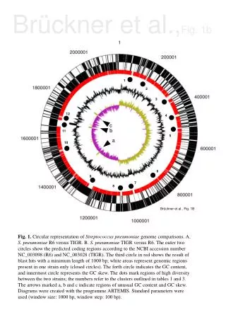
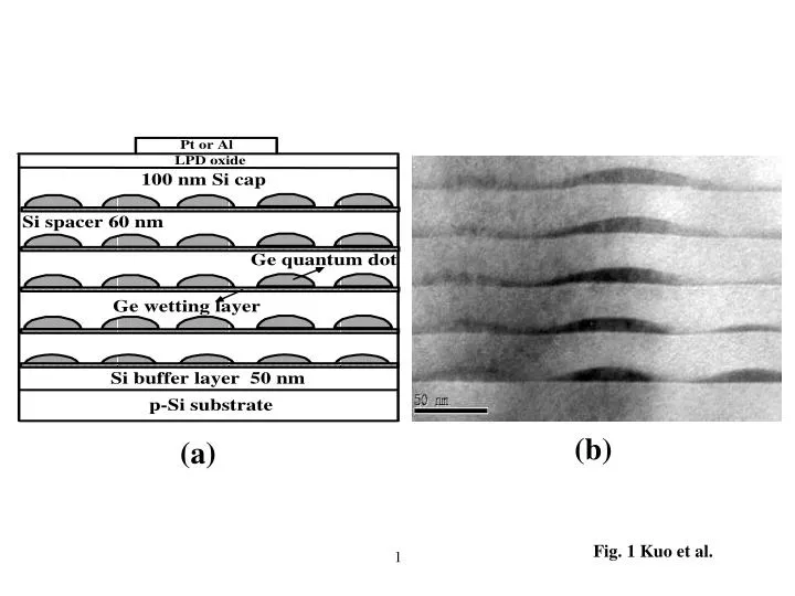
(b) (a) Fig. 1 Kuo et al.
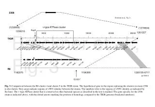
(b) (a) Fig. 3 . Kuo et al.
TEM of epi Ge before PMA : After PMA : Pt Germanide Ref :IEEE ELECTRON DEVICE LETTERS JohnY. Spann, Student Member, IEEE, Robert A. Anderson, Student Member, IEEE, Trevor J. Thornton, Member, IEEE, Gari Harris, Member, IEEE, Shawn G. Thomas, Member, IEEE, and Clarence Tracy
Pt SB w/ epi Ge/Si From MinHung
N-type Si EFm EFn EFm N-type Si EFn
I-V curves thermionic emission tunneling current Thermionic-field emission (Tunneling) Thermionic emission
Thermionic-field emission (Tunneling) Thermionic emission From Simulation : nSi E-field~ 2e4 V/cm Epi Ge E-field~ 3e6 V/cm
C-V calibration : epi Ge with cap : From I-V • So I just show the C-V before -2V for epi Ge with cap Pt SBD.
SBD C-V : EFm N-type Si EFn • Epi Ge with cap for SBD has higher C than Bulk nSi and epi Ge w/o cap.
Floating gate Memory : Nano-crystals memory (Freescale) : Leakage path Leakage path Disadvantage : • Smaller dot size for scaling. • Scaling (SiO2 gap between dots must exceed 5 nm) • Charge loss in full floating gate. Thick tunnel oxide. • Trade-off between erase speed and tunnel oxide thickness – charge leaks off from the floating gate. • The reliability issue when scaled down to deep submicron.
Trap Memory : • Advantage : • Trap size = atom for scaling • ∆VT can be large if trap density is height • After annealing, Si implanted into the SiO2 separates from the oxide phase and form the Si-NCs.
Schematic energy band diagram under program/erase Program/erase performance is enhanced using high-k blocking oxide.
Glue Al gate Al2O3~10nm Al2O3~10 nm HfAlO~10nm HfO2~5.2 nm p-Si SiO2~3.6 nm SiO2~3nm p-Si 10 nm TEM characteristics All high-k films are deposited by ALD. After annealing treatment (1000oC, 10s) in N2 ambient, HfAlO film shows partial crystalline, while HfO2 film shows fully crystalline. The Al2O3 film shows also partial crystalline.
C-V hysteresis memory window Structure: SiO2(3nm)/HfO2(10nm)/Al2O3(10nm) Al gate electrode Frequency: 100kHz Ramp rate: 0.1V/s A good C-V hysteresis memory window of high-k charge trapping layers is observed with high gate voltage. The memory window is slightly lower (7-8V@Vg=15V) as compared with reported data (~10V@Vg=12V) on TaN/AlLaO3(12nm)/AlGaN(10nm)/SiO2 (2.7nm)/p-Si [A. Chin et al., 2005 IEDM Tech. Dig. P. 165].