Download
1 / 1
10 likes | 182 Views
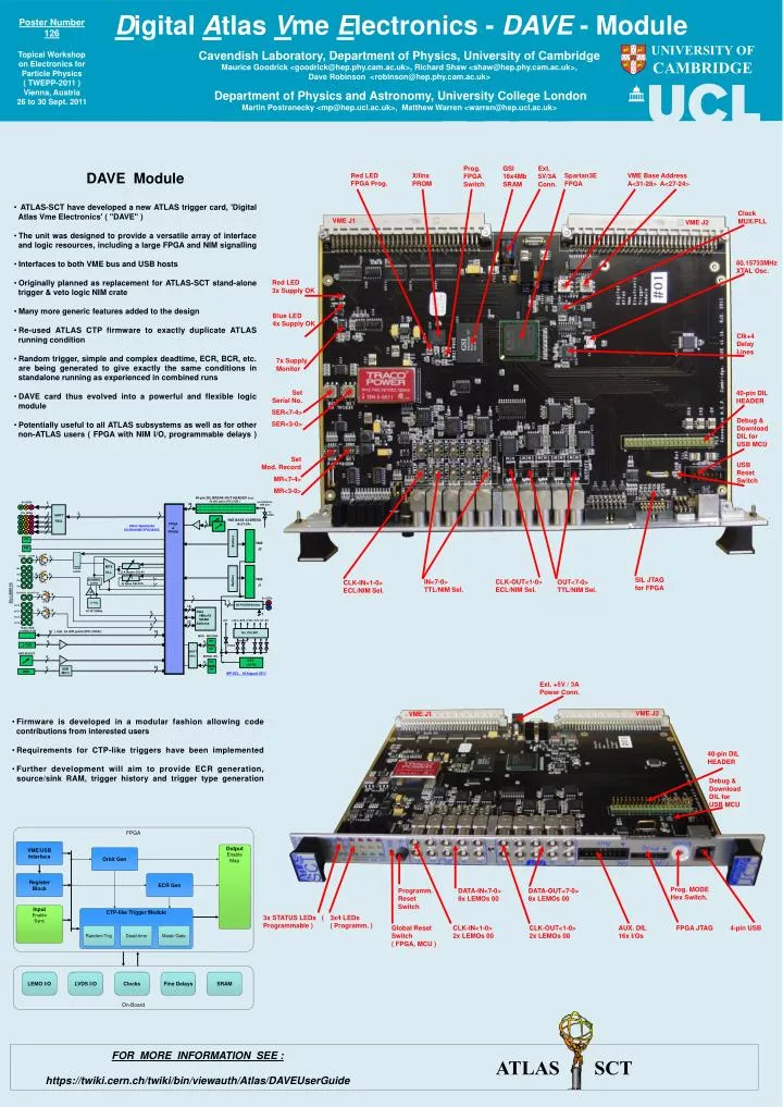
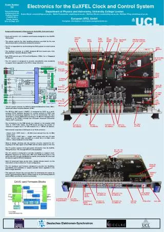
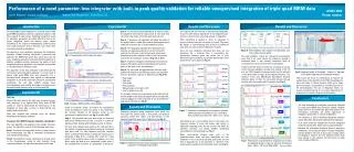
40-pin DIL BREAK-OUT HEADER (incl. 4x diff. pairs 2V5 LVDS ). 3. 6x POWER 2x GND pins. 3x LEDs. D igital A tlas V me E lectronics - DAVE - Module. Poster Number 126 Topical Workshop on Electronics for Particle Physics ( TWEPP-2011 ) Vienna, Austria 26 to 30 Sept. 2011.

E N D
40-pin DIL BREAK-OUT HEADER (incl. 4x diff. pairs 2V5 LVDS ) 3 6x POWER 2x GND pins 3x LEDs Digital Atlas Vme Electronics - DAVE - Module Poster Number 126 Topical Workshop on Electronics for Particle Physics ( TWEPP-2011 ) Vienna, Austria 26 to 30 Sept. 2011 6x FUSES 3 8 8 7 16 4 8 22 2 7 24 2 6 16 32 2 8 4 8 12x LEDs SHIFT REG. 3 VME BASE ADDRESS A<31-24> FPGA FPGA & PROM 3 Xilinx Spartan3e XC3S1600E-5FGG400C 3 VME/USB Interface Output Enable Map Orbit Gen UNIVERSITY OFCAMBRIDGE Buffers SW SW SW SW SW SW VME J2 Cavendish Laboratory, Department of Physics, University of CambridgeMaurice Goodrick <goodrick@hep.phy.cam.ac.uk>, Richard Shaw <shaw@hep.phy.cam.ac.uk>, Dave Robinson <robinson@hep.phy.cam.ac.uk> Department of Physics and Astronomy, University College LondonMartinPostranecky <mp@hep.ucl.ac.uk>, Matthew Warren <warren@hep.ucl.ac.uk> Register Block ECR Gen NIM ECL CLKIN0 CLKIN1 2 2 MPX PLL CLKIN select IN0 NIM TTL CLK Master DELAY 8 8 Input Enable Sync IN2 20x LEMO-00 CTP-like Trigger Module 4 4 VME J1 40/80MHz select Buffers IN4 4x Slave DELAYS 4 IN6 Random Trig Dead-time Mask/ Gate :2 NIM ECL CLKOUT0 CLKOUT1 2 2 2x LEDs X-TAL 80.15733MHz All POWER Monitor OUT0 NIM TTL 8 8 Data 4Mbx18 SRAM Address OUT2 7 On-Board OUT4 LEMO I/O LVDS I/O Clocks Fine Delays SRAM +5V +3V3 +2V5 +1V8 +1V2 -5V -2V OUT6 16-pin AUX. CONNECTOR 16 ( incl. 2x diff. pairs 2V5 LVDS ) 6x DC-DC MOD. RECORD J-TAG FUSES USB SHIFT REG. HEX SELECT SERIAL NO. EXT. +5V IN USB MCU • DAVE Module • ATLAS-SCT have developed a new ATLAS trigger card, 'Digital • Atlas Vme Electronics' ( "DAVE" ) • The unit was designed to provide a versatile array of interface • and logic resources, including a large FPGA and NIM signalling • Interfaces to both VME bus and USB hosts • Originally planned as replacement for ATLAS-SCT stand-alone • trigger & veto logic NIM crate • Many more generic features added to the design • Re-used ATLAS CTP firmware to exactly duplicate ATLAS • running condition • Random trigger, simple and complex deadtime, ECR, BCR, etc. are being generated to give exactly the same conditions in • standalone running as experienced in combined runs • DAVE card thus evolved into a powerful and flexible logic • module • Potentially useful to all ATLAS subsystems as well as for other • non-ATLAS users ( FPGA with NIM I/O, programmable delays ) MP-UCL, 18 August 2011 Prog. FPGA Switch GSI 18x4Mb SRAM Ext. 5V/3A Conn. Red LED FPGA Prog. Xilinx PROM Spartan3E FPGA VME Base Address A<31-28> A<27-24> Clock MUX/PLL VME J1 VME J2 80.15733MHz XTAL Osc. Red LED 3x Supply OK Blue LED 4x Supply OK Clk+4 Delay Lines 7x Supply Monitor Set Serial No. SER<7-4> SER<3-0> 40-pin DIL HEADER Debug & DownloadDIL for USB MCU Set Mod. Record MR<7-4> MR<3-0> USB Reset Switch SIL JTAG for FPGA IN<7-0> TTL/NIM Sel. CLK-OUT<1-0> ECL/NIM Sel. OUT<7-0> TTL/NIM Sel. CLK-IN<1-0> ECL/NIM Sel. • Firmware is developed in a modular fashion allowing code • contributions from interested users • Requirements for CTP-like triggers have been implemented • Further development will aim to provide ECR generation, source/sink RAM, trigger history and trigger type generation Ext. +5V / 3A Power Conn. VME J2 VME J1 40-pin DIL HEADER Debug & Download DIL for USB MCU Prog. MODE Hex Switch. Programm. Reset Switch DATA-IN<7-0> 8x LEMOs 00 DATA-OUT<7-0> 8x LEMOs 00 3x STATUS LEDs ( Programmable ) 3x4 LEDs ( Programm. ) Global Reset Switch ( FPGA, MCU ) CLK-IN<1-0> 2x LEMOs 00 CLK-OUT<1-0> 2x LEMOs 00 AUX. DIL 16x I/Os FPGA JTAG 4-pin USB FOR MORE INFORMATION SEE : https://twiki.cern.ch/twiki/bin/viewauth/Atlas/DAVEUserGuide ATLAS SCT


![[INSERT] Poster number (eg P324, or OP212). Title of your poster.](https://cdn3.slideserve.com/6811451/slide1-dt.jpg)