Download
1 / 42
420 likes | 548 Views
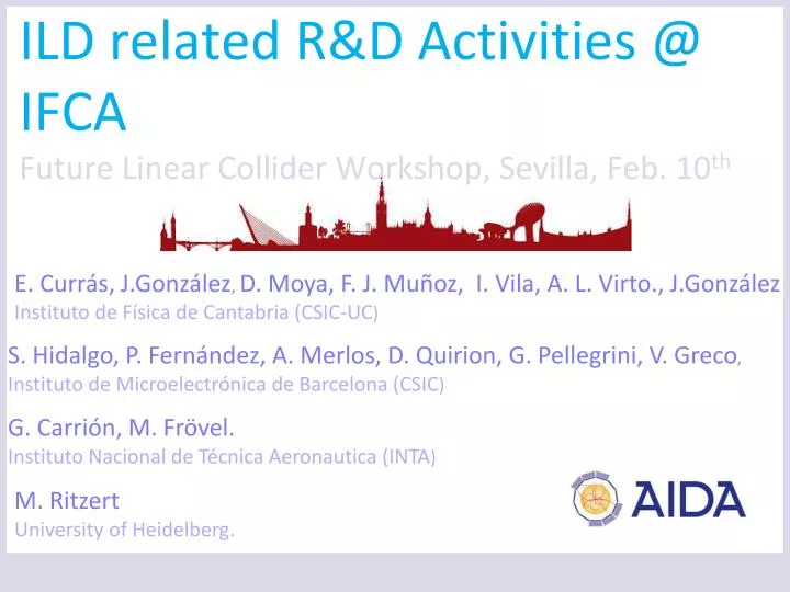
ILD related R&D Activities @ IFCA F uture Linear Collider Workshop, Sevilla , Feb. 10 th. E. Currás , J.González , D . Moya , F. J. Muñoz, I. Vila, A. L. Virto ., J.González Instituto de Física de Cantabria ( CSIC-UC ).

E N D
ILD related R&D Activities @ IFCA Future Linear Collider Workshop, Sevilla, Feb. 10th E. Currás, J.González, D. Moya, F. J. Muñoz, I. Vila, A. L. Virto., J.González Instituto de Física de Cantabria (CSIC-UC) S. Hidalgo, P. Fernández, A. Merlos, D. Quirion, G. Pellegrini, V. Greco, Instituto de Microelectrónica de Barcelona (CSIC) G. Carrión, M. Frövel. • InstitutoNacional de TécnicaAeronautica (INTA) M. Ritzert • University of Heidelberg.
Outline • A structural and environmental monitor for Belle-2 vertex detector based on Fiber Optic Sensor (FOS) • R&D on microstrips sensors (resistive & low signal gain) ivan.vila@csic.es, 5th PXD-SVD Joint Workshop, January 22-24,2013, DESY.
FOS Monitor ivan.vila@csic.es, 5th PXD-SVD Joint Workshop, January 22-24,2013, DESY.
L-shapebasics • Temperature & strain to displacement transducer with custom geometry for integration in PXD • Readout speed from zero to 1KHz (vibrations) • Currently three demonstrators manufactured Contactsurface Lockedpart FBG sensors Contactball ivan.vila@csic.es, 13th DEPFET Workshop, June 12-15h,2013, RingBerg.
L-ShapeDemostrators OnemillimiterDiameterQuartzcontactball Clampingsystem ballglued L-shapetip ivan.vila@csic.es, 13th DEPFET Workshop, June 12-15h,2013, RingBerg.
, FOS Monitor Timeline • 2009 Oct FOS Monitor proposal • 2010 Jan Omega-shape proposal • 2010 Oct. FOS radiation hardness study (1.5 GRads ,3.3 1015 p/cm2) • 2011 January First omega mechanical dummies • 2011 Sept. FOS radiation hardness study ( 10 Mrads ) • 2011 Dec Proof-of-concept-prototype omega • 2012 Feb Omega calibration. • 2012 March New transducer design L-shape • 2012 May Test in depfet mock-up at IFIC • 2012 October L –shape calibration (resolution less 1 um ,accuracy≈10 um ) • 2013 May Test in mock-up at IFIC (N2 atmosphere) • 2014 January commissioning at PXD-SVD common test beam D.Moya, LC2013 Tracking-Vertex session, Desy May. 30th 2013
Thermal calibrations & temperature compensation • Calibration using a SIKA thermocouples calibrator. • The sensitivity of three sensors was constant and near the same (difference<0.6%) Maximumdeviation < 3 pm (0.3 ºC) Error X 10 Error X 10 Error X 10 • Trivial approach to temperature compensation ivan.vila@csic.es, 13th DEPFET Workshop, June 12-15h,2013, RingBerg.
DisplacementCalibration • Displacement measured with Michelson interferometer for high precision calibration (tenth of a micron) • Readout of L-shape compared with true position (interferometer) Contactball Micrometricstage Contact surface L-shape D.Moya, LC2013 Tracking-Vertex session, Desy May. 30th 2013 ivan.vila@csic.es, 13th DEPFET Workshop, June 12-15h,2013, RingBerg.
L-shape Output Stability • Short term studies (temperature constant ± 0.1° ) • Continuous readout of the sensor output. • Stabilities below or about 1um (convolution with mechanics stability) RMS ≈ 1.1 um RMS ≈ 0.6 um ivan.vila@csic.es, 13th DEPFET Workshop, June 12-15h,2013, RingBerg.
L-shapeLinearity vs. Displacement • Calibration over a range of 1mm • Resolution (readout resolution) 0.5 um. • Accuracy (diff. Between inter & L-shape) ≈ 2 um Sensitivity 1.2 pm/um ivan.vila@csic.es, 13th DEPFET Workshop, June 12-15h,2013, RingBerg.
PXD – SVD Integrated test beam ivan.vila@csic.es, 5th PXD-SVD Joint Workshop, January 22-24,2013, DESY.
PXD – SVD Integrated test beam ivan.vila@csic.es, 5th PXD-SVD Joint Workshop, January 22-24,2013, DESY.
FOS Monitor: FOS Packing ivan.vila@csic.es, 5th PXD-SVD Joint Workshop, January 22-24,2013, DESY.
FOS Monitor: DAQ – SC integration • Optical routing of the sensors up to the interrogating units • Readout integrated in EPICS (dedicated driver over Ethernet ). The integration went very smooth ready since the January 6th ivan.vila@csic.es, 5th PXD-SVD Joint Workshop, January 22-24,2013, DESY.
FOS Monitor: Data: MARCO in-let & out-let lines Zero degrees cooling ivan.vila@csic.es, 5th PXD-SVD Joint Workshop, January 22-24,2013, DESY.
FOS Monitor Data: Ambient Temp Zero degrees cooling ivan.vila@csic.es, 5th PXD-SVD Joint Workshop, January 22-24,2013, DESY.
FOS Monitor: Ambient Temp+%RH N2 injection ivan.vila@csic.es, 5th PXD-SVD Joint Workshop, January 22-24,2013, DESY.
FOS Monitor:Humidity measurements • Comparing the wavelength shift of ambient sensors (naked fibers) vs. commercial Humidity sensors inside the dry box. • Excellent linearity and sensibility after temperature compensation ivan.vila@csic.es, 5th PXD-SVD Joint Workshop, January 22-24,2013, DESY.
Conclusions • A FOS-based temperature and humidity monitor read-out through EPICS commissioned and running smoothly since the beginning of the test beam. • Most of the R&D activities required for the implementation of FOS monitor (environmental and displacement) are completed. Still some more “academic “ loose ends to be completed this year. • Next: System-wise activities for mechanical integration in Belle-II. ivan.vila@csic.es, 5th PXD-SVD Joint Workshop, January 22-24,2013, DESY.
PART 2 - R&D ON MICROSTRIPS • Microstrip sensors with resistive electrodes. • Low Gain Microstrip Sensors. ivan.vila@csic.es, 5th PXD-SVD Joint Workshop, January 22-24,2013, DESY.
R&DMotivation • Charge division in microstrips: • Long microstrips ladders (several tens of centimeters) proposed for the ILC tracking detectors. • Getting the particle hit coordinate along the strip using the charge division method. • Avoid the complexity of double sided sensors and the additional material of a second layer of sensors. • Low gain segmented p-type pixels (strips) • Implementing a small gain in the segmented diode so we can reduce the thickness of the sensors without reducing the signal amplitude • Smaller contribution to the material budget. E. Currás - LC Workshop 27-31 May 2013, DESY
S1 S1 with resistive coupling electrodes. Y-coordinate: Resistive charge division method. Resistive material Aluminium Aluminium y x x ** Electrode resistance >> preamplifier impedance. L L S1=f(y) S2=f(L-y) y A2 L A1+A2 = Resistive material: high doped polysilicon ** V. Radeka, IEEE Transaction on Nuclear Science NS-21 (1974) 51 S2 ChargeDivision in uStrips Simple single-side AC-coupled microstrip detectors X-coordinate: cluster-finding algorithms for strip detectors. E. Currás - LC Workshop 27-31 May 2013, DESY
Proof-of-Concept Prototype 2 Beetle chips ALIBAVA DAQ system for microstrip detectors, based on the Beetle analogue readout ASIC 3D axis stage with displacement accuracy ≈ 10 μm • Pulsed DFB laser λ=1060nm • Gaussian beam spot width ≈ 15 μm • pulse duration 2ns • 256 channels • peaking time = 25ns • S/N≈20 for standard no irradiated detectors Clean room laboratory at IFCA, Santander E. Currás - LC Workshop 27-31 May 2013, DESY
EquivalentElectricalCircuit Detector (p+-on-n) model *** 80 cells 250 μm long p e- h+ Vbias Peaking time 25ns (Beetle chip ALIBAVA DAQ system). • rise time 2ns • Q~4fC E. Currás - LC Workshop 27-31 May 2013, DESY
S1 S2 Particle t t t2 t1 V SignalPropagation– Linearity (Simulation) S1 2 mm y S2 18 mm E. Currás - LC Workshop 27-31 May 2013, DESY
R/l=2.8 Ω/μm R/l=12.2 Ω/μm 20000 events ∀ measurement Systematic error => Ballistic deficit E. Currás - LC Workshop 27-31 May 2013, DESY
A2 A1+A2 R/l=2.8 Ω/μm R/l=12.2 Ω/μm Longitudinal spatial resolution for 6 MIPs signal 1.1% L => 220 μm 1.2% L => 240 μm σA1=1.83 ADU σA2=1.80 ADU E. Currás - LC Workshop 27-31 May 2013, DESY
Test Beam Characterization • Test beam at CERN SPS Pion Beam, Nov 2012 • Firstsuccessfulintegration and synchronizationwith AIDA MIMOSA pixel telescope • Prelimiraryresults: • Monitoring of beamprofile. • Currently in progress: • Efficiency and resolutionusing tracking information. E. Currás - LC Workshop 27-31 May 2013, DESY
Vista frontal del setup a escala (aproximada) Transparente Mimosa Haz RMS de 12 mm Poly
s/n test beam vs s/n radioctivesource Resistivestrips detector Conventionalstrips detector E. Currás - LC Workshop 27-31 May 2013, DESY
Tracking (Telescopio) Proyección plano DUT Distribución del número de trazas Totales por evento del telescopio en el plano del DUT Trazas del telescopio proyectadas en el plano del DUT
Tracking (PolyA) Distribución del número de clusters Detectados en el DUT: Corte de 4 y 2 sigmas No hay corte en tiempo 0-100 ns Con un corte de 20-40 ns(selecciono el pico), no varían las resoluciones.
Y resolution (logitudinal) Se usan sólo los clusters que machean previamente el la posición transversal, Se toma un corte de 5 sigmas (0.025 mm).
Summary • In terms of position resolution the sensors behaves as predicted. Is it enough ? • No result on efficiency due to problems with the timing sensor and wrong sensor biasing. ivan.vila@csic.es, 5th PXD-SVD Joint Workshop, January 22-24,2013, DESY.
SEGMENTED P-TYPESENSORSWITHCHARGEAMPLIFICATION E. Currás - LC Workshop 27-31 May 2013, DESY
Charge Multiplication- pixel detectors We are starting the fabrication of new p-type pixel detectors with enhanced multiplication effect in the n-type electrodes, very low collection times and with no cross-talk. Three different approaches: • Thin p-type epitaxyal substrates • Low gain avalanche detectors • 3D with enhanced electric field. Two projects funded by CERN RD50 collaboration to work on these technologies. http://rd50.web.cern.ch/rd50/ E. Currás - LC Workshop 27-31 May 2013, DESY
Low gain avalanche detectors (LGAD) N+ Implating an n++/p+/p- junction along the centre of the electrodes. Under reverse bias conditions, a high electric field region is created at this localised region, which can lead to a multiplication mechanism (impact Ionization). High Electric Field region leading to multiplication Advantages = Thinning while keeping same S/N as standard detectors. P 285 um P. Fernandez et al, “Simulation of new p-type strip detectors with trench to enhance the charge multiplication effect in the n-type electrodes” , Nuclear InstrumentsandMethodsinPhysicsResearchA658(2011) 98–102. E. Currás - LC Workshop 27-31 May 2013, DESY
Simulation of the Electric Field - To obtain the manufacture parameters (doping profiles) Standard Strip Strip with P-type diffusion Strip with P-type diffusion: 2D and 1D doping profiles E. Currás - LC Workshop 27-31 May 2013, DESY
Red laser TCTcharacterization Bottominjection Standard diode n on p P-type diffusion diode 5ns 285 um h+ e- Red laser (1060 nm) E. Currás - LC Workshop 27-31 May 2013, DESY
Red laser TCT characterization Chargecollectionefficiency Standard diode P-type diffusion diode E. Currás - LC Workshop 27-31 May 2013, DESY
GRACIAS ! ivan.vila@csic.es, 5th PXD-SVD Joint Workshop, January 22-24,2013, DESY.