Download
1 / 18
180 likes | 498 Views
Combinational Logic Design. COE 202 Digital Logic Design Dr. Aiman El-Maleh College of Computer Sciences and Engineering King Fahd University of Petroleum and Minerals. Outline. Combinational Logic Circuits Combinational Circuits Design Procedure Design Examples

E N D
Combinational Logic Design COE 202 Digital Logic Design Dr. Aiman El-Maleh College of Computer Sciences and Engineering King Fahd University of Petroleum and Minerals
Outline • Combinational Logic Circuits • Combinational Circuits Design Procedure • Design Examples • BCD to Excess 3 Code Converter • BCD to 7-Segment Decoder for LED
Combinational Logic Circuits • A combinational logic circuit has: • A set of m Boolean inputs, • A set of n Boolean outputs, and • n logic functions, each mapping the 2m input combinations to an output • Outputs are determined only by present inputs Each Output = F (the m inputs)
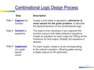
Combinational Circuits Design Procedure • 1. Specification (Requirement) • Write a specification for what the circuit should do e.g. add two 4-bit binary numbers • Specify names for the inputs and outputs • 2. Formulation • Convert the Specification into a form that can be Optimized • Usually as a truth table or a set of Boolean equations that define the required relationships between the inputs and outputs • 3. Logic Optimization • Apply logic optimization (2-level & multi-level) to minimize the logic circuit • Provide a logic diagram or a netlist for the resulting circuit using ANDs, ORs, and inverters
Combinational Circuits Design Procedure • 4. Technology Mapping and Design Optimization • Map the logic diagram or netlist to the implementation technology and gate type selected, e.g. CMOS NANDs • Perform design optimizations of gate costs, gate delays, fan-outs, power consumption, etc. • Sometimes this stage is merged with stage 3 • 5. Verification • Verify that the final design satisfies the original specification- Two methods: • Manual: Ensure that the truth table for the final technology-mapped circuit is identical to the truth table derived from specifications • By Simulation: Simulate the final technology-mapped circuit on a CAD tool and test it to verify that it gives the desired outputs at the specified inputs and meets delay specs etc.
BCD to Excess 3 Code Converter • 1. Specification • Transforms BCD code for the decimal digits (0-9) to the corresponding Excess-3 code • BCD code words for digits 0 through 9: 4-bit patterns 0000 to 1001, respectively • Excess-3 code words for digits 0 through 9: 4-bit patterns obtained by adding 3 (binary 0011) to each BCD code input • 2. Formulation • In the form of a truth table: Variables • BCD: A,B,C,D Excess-3: W,X,Y,Z • Don’t Cares: BCD 1010to 1111
BCD to Excess 3 Code Converter Z map Y map • 3. Optimization • 2-level usingK-maps C C z 1 1 1 1 0 1 3 2 0 1 3 2 1 1 1 1 4 5 7 6 4 5 7 6 B B X X X X X X X X 12 13 15 14 12 13 15 14 A A 1 X X 1 X X 8 9 11 10 8 9 11 10 D D W map X map C C 1 1 1 0 1 3 2 0 1 3 2 1 1 1 1 4 5 7 6 4 5 7 6 B B X X X X X X X X 12 13 15 14 12 13 15 14 A A 1 X X 1 1 X X 8 9 11 10 8 9 11 10 D D
BCD to Excess 3 Code Converter • 3. Logic Optimization (continued) • Start with SOPs (2-level) from the K-maps: • Extractinga common factor:
A W B X Y C D Z BCD to Excess 3 Code Converter • 4. Technology Mapping • Use a library containing inverters, 2-input NAND, 2-input NOR, and 2-2 AOI gates T1 T1
BCD to Excess 3 Code Converter • 5. Verification • Find the SOP Boolean equations from the final technology mapped circuit • Find the truth table from these equations • Compare it with the specification truth table • Finding the Boolean Equations T1
BCD to Excess 3 Code Converter • 5. Verification- Manual, Continued: The circuit truth table from the equations - Compare it with the specification truth table: The tables match!
BCD to Excess 3 Code Converter • 5. Verification- by Simulation: Procedure • Use a schematic editor or text editor to enter a gate level representation of the final circuit • Use a waveform editor or text editor to enter a test consisting of a sequence of input combinations to be applied to the circuit • This test should guarantee the correctness of the circuit if the simulated responses to it are correct • Generation of such a test can be difficult, and sometimes people apply all possible “care” input combinations
BCD to Excess 3 Code Converter • 5. Verification- by Simulation: Final Circuit Schematic
BCD to Excess 3 Code Converter • Run the simulation of the circuit for 120 ns • Do the simulation output combinations match the original specification truth table?
BCD to 7-Segment Decoder for LED • 1. Specification • Transforms a BCD input code for the decimal digits (0 to 9) to 7 outputs (one for each of the seven LED segments) used to drive the display • Each output indicates whether the corresponding segment is ON (1) or OFF (0) for the input BCD code
BCD to 7-Segment Decoder for LED • 2. Formulation • 4 Input Variables • BCD: A,B,C,D (LSB) • 7 Output Variables • Drivers for the 7 Segments: a,b,c,d,e,f,g • (1 = segment lit, i.e. active high) • Don’t Cares • None! Display is OFF for non BCD codes
BCD to 7-Segment Decoder for LED • 3. Optimization: Using Seven 4-Variable K-maps we get: