Download
1 / 43
2.68k likes | 5.2k Views
Introduction to Thin Film Technology. H. Shirinzadeh Semiconductors and Device Fabrication. End.

E N D
Introduction to Thin Film Technology H. Shirinzadeh Semiconductors and Device Fabrication End
Course ObjectivesThis course will provide a thin film deposition methods, their possibilities and limitations. Hands-on demonstrations and experiments in the our Laboratories will help the participants to better understand the possibilities of each deposition method and stimulate informal discussions between participants and experts. Essential fundamental aspects, as well as the technology of thin-film growth from the vapor phase - evaporation, PVD and CVD, etc, it will help us to learn how to test and characterize film structure and related properties after deposition
TECHNOLOGY FOCUS • Thin film technology is pervasive in many applications, including microelectronics, optics, magnetic, hard resistant coatings, micro-mechanics, etc. • Progress in each of these areas depends upon the ability to selectively and controllably deposit thin films - thickness ranging from tens of ångströms to micrometers - with specified physical properties. • its requires control - often at the atomic level - of film microstructure and microchemistry. There are a vast number of deposition methods available and in use today. • all methods have their specific limitations and involve compromises with respect to process specifics, • substrate material limitations, expected film properties, and cost. This makes it difficult to select the best technique for any specific application.
Coating Processesتكنولوژي لايه نازك Electro deposition Spraying Chemical coating Welding Conversion coating Molecular beam epitaxy Vapour deposition Chemical vapour deposition Physical vapour deposition Back
Advantages Low temperature treatment High hardness Low friction Applicable to a wide range of metal substrates Thick layers possible Disadvantages Poor thickness uniformity on complex components Hydrogen embrittlement Not applicable to insulating substrates Possible environmental concerns with plating baths Elecrochemical deposition Back
Advantages Low temperature treatment More corrosion resistant than electrodeposited chromium Can coat complex shapes uniformly Hard particles can be incorporated to increase hardness PTFE can be incorporated to reduce friction Can coat most metals and some insulators Disadvantages More expensive than electroplated chromium Heat treatment is needed to develop optimum properties Chemical Coatings Back
Thin compound layers can be produced by reacting a metal surface with an acidic solution. e.g. Thin (10mm) coatings of metal phosphates are formed on steel substrates exposed to phosphoric acid. These provide low friction surfaces with some resistance to adhesive wear. Often used to help components run-in. Advantages Cheap and simple to perform Low temperature treatment Disadvantages Restricted range of materials can be treated Thin treated layer Poor treatment durability Difficult to control treatment quality on heterogeneous materials Conversion Coatings Back
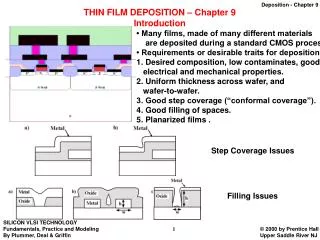
Gaseous compounds react to form a dense layer on a heated substrate. The most widely deposited wear-resistant coatings are TiC, TiN, chromium carbide and alumina. Deposition temperatures are generally in the range 800-1000°C which restricts the range of materials which can be coated and can lead to component distortion. Thicknesses are limited to about 10mm due to the thermal expansion mismatch stresses which develop on cooling which also restrict the coating of sharp edged components. Advantages High coating hardness Good adhesion (if the coating is not too thick) Good throwing power (i.e. uniformity of coating) Disadvantages High temperature process (distortion) Sharp edge coating is difficult (thermal expansion mismatch stresses) Limited range of materials can be coated Environmental concerns about process gases Chemical Vapour Deposition (CVD) Back
Advantages Excellent process control Low deposition temperature Dense, adherent coatings Elemental, alloy and compound coatings possible Disadvantages Vacuum processes with high capital cost Limited component size treatable Relatively low coating rates Poor throwing power without manipulation of components low pressure coating processes in which the coating flux is produced by a physical process. There are two main types:- Evaporation Sputtering In both cases the source material is a solid (metal or ceramic). A reactive gas may be used in the deposition chamber to deposit compound coatings from an elemental source or maintain the stoichiometry of coatings from compound sources. Typical coating thicknesses range from 1-10mm for wear-resistant coatings, though thinner layers are used in microelectronics and thicker layers are used for high temperature corrosion protection of gas turbine components. Physical Vapour Deposition (PVD) Back
Evaporation Processes The vapour pressure of most materials increases with temperature and if it exceeds the ambient pressure the material will rapidly evaporate into the environment. In a coating chamber the pressure is reduced and the source material heated until a desired vapour flux is maintained which is controlled by the source material, the source temperature and the system pressure. Heating can be performed in several ways:- • Resistive heating (e.g. aluminium evaporation from TiB2 boat) • Electron beam evaporation (e.g. metals such as tungsten) • Cathodic arc evaporation (e.g. titanium evaporation for TiN coatings) The vapour pressures of different metals vary over several orders of magnitude so it is difficult to evaporate alloys and control composition. As-deposited evaporated coatings are porous due to the limited mobility of coating atoms on component surfaces. This can be controlled by heating or ion plating (see later) Spatter from localised boiling can lead to droplet formation which affects coating performance Back
Main sputtering processes:- DC diode sputtering (for conducting targets) RF sputtering (for insulating targets) When energetic ions strike a surface, material is ejected by the transfer of momentum from the ion to the target atoms (akin to billiard ball collisions at the atomic scale). This can be conveniently achieved in a low pressure glow discharge of an inert gas such as argon. In such a process the target material is made the cathode and is raised to a potential of several hundred volts. Electrons leaving the cathode stream out into the gas phase where they can impact with argon atoms, ionising them. The positively charged argon is then accelerated to the cathode where it impacts and sputters away material. The sputtering yields of different elements for given impact conditions do not vary very much so target alloy compositions can be maintained in the coating except in cases where there are large differences in the atomic weights of alloy constituents. Sputtering Processes Back The coating rate scales with the electrical power used to sustain the discharge. The coating rate also depends on the plasma density, so techniques to increase this (e.g. by confining the electrons close to the target using magnets) will increase the coating rate. However, as much as 95% of the power is dissipated as heat in the target so good cooling is essential.
Advantages Low temperature process Very versatile - every stable element in the periodic table can be implanted into any vacuum compatible target Highly controlled No distortion - can be applied to finished components Not a coating process Disadvantages Line of sight process Expensive vacuum equipment needed Very thin treated layer A vacuum process in which a beam of ions is directed at the surface and injected into it. The ions lose energy in collisions with the target atoms and come to rest in the surface layer of the material with an approximately Gaussian distribution. The ion penetration depth depends on the ion species, ion energy and target material, bur is generally less than 1mm. For steels the main ion used is nitrogen, which hardens the surface by forming nitride precipitates and solid solutions. The damage introduced by the implantation process also introduced a compressive residual stress which improves fatigue performance. Ion Implantation • Ion implantation is routinely used for semiconductor doping and treatment of expensive plastics injection moulding tools where any wear is detrimental.
Advantages Cheap Applicable to large components Localised coating possible Excellent adhesion Disadvantages Limited range of coating materials Minimum thickness limits The same methods which can be used for joining materials can be used to deposit wear resistant coatings (hardfacings). Coating materials range from low alloy steels to tungsten carbide composites. High deposition rates are possible and very thick coatings can be produced. It is impractical to produce layers less than 2-3mm thick. There can be problems with cracks in weld deposits Welding Processes Back
Thermal Evaporation in Vacuum: From Source to Substrate we will first discuss the thermal evaporation parameters, such as vapor pressure, evaporation rates and directionality. This will be followed by a technical description of various types of evaporation sources, both resistively heated and electron beam heated.We will then discuss how to monitor and control the evaporation processes, with emphasis especially on in-process techniques. Boats FilamentsBoats Back
Crucible Heaters Boats FilamentsBoats Back
Solar Cell Technologies Solar Cell Technologies Introduction Three key elements in a solar cell form the basis of their manufacturing technology. The first is the semiconductor, which absorbs light and converts it into electron-hole pairs. The second is the semiconductor junction, which separates the photo-generated carriers (electrons and holes), and the third is the contacts on the front and back of the cell that allow the current to flow to the external circuit. The two main categories of technology are defined by the choice of the semiconductor: either crystalline silicon in a wafer form or thin films of other materials. Back
سلولهاي خورشيدي نوع سيليكون 1- سلولهاي خورشيدي ازتك بلور سيليكان 4- سلولهاي خورشيدي نوع سيليكون از طريق لايه هاي نازك 2- سلولهاي خورشيدي ازپلي كريستال سيليكون 3 - سلولهاي خورشيدي نوع آمورف سيليكان
- سلولهاي خورشيدي ازتك بلور سيليكان ساخت سلولهاي خورشيدي ازتك بلور سيليكان بدون عيوب كريستالي و با كمترين مقدار مجاز (محل خالي) حاتز اهميت مي باشد.Dislocation روشهاي رايج در اشل صنعتي 1- روش چكرالسكي 2 - بريجمن 3- ذوب منطقه اي Back
سلولهاي خورشيدي ازتك بلور سيليكان در اين روش سيليكون در ظروفي از جنس كوارتز ٌٌRF ريخته و توسط كوره هاي الكتريكي يا (راديو فركانس) ذوب و به كمك تخمك سيليكون تمام ذوب را به آهستكي به سمت بالا كشند(Seed) روشهاي رايج در اشل صنعتي Back
سلولهاي خورشيدي ازپلي كريستالسيليكون اگرسيليكون را در شرايط نرمال در بوته هاي گرافيت ذوب و همراه گاز آرگون خنك نمايند.سيليكون از كريستالهاي ريز ميكروسكوپيك تشكيل ميشود ، اگر شرايط خنك كردن به تدريج و خيلي آهسته باشد كريستالهاي ريز امكان بزرگ شدن را پيدا مي نمايند كه به اين محصول پلي كريستال سيليكون مي گويند كه اندازه كريستاليزه شدن دانه ها بستگي به شرايط خنك شدن انجماد دارد. پلي كريستال سيليكون را مي توان بصورت هاي گوناگون از قبيل استوانه اي، مكعب مستطل، نواري و يا ودقه اي نازك از حمام مذاب باكيفيت عالي رشد داد. سلولهاي خورشيدي ازپلي كريستال داراي بازدهي 10-12% مي باشند Back
سلولهاي خورشيدي نوع آمورف سيليكان سيليكون به صورت آمورف ( بي شكل) مي توانند يكي از پروسه هاي ساخت سلولهاي خورشيدي باشد. آمورف سيليكون را توسط سيستمهاي تبخير و پلاسما اسپري تهيه نمود. آمورف سيليكون داراي خواس فيزيكي كريستالين نمي باشد و همين علت در موقع تشكل، اتمهاي آن بصورت اتفاقي و بي نظم و ترتيب توزيع و قرار مي گيرد. Back
Electronbeam Deposition Systems Vacuum : 5X10⁻⁷ torr Multi source: 4 – 6 S Power : 4 – 6 Kev In-situ electrical measurements Back
- سلولهاي خورشيدي نوع سيليكون از طريق لايه هاي نازك اين نوع سلولها خورشيدي با خلوص بالا از طريقسييستمهاي تبخير از فاز مذاب به روشهاي 1.Molecular beam Epitaxy and 2.Electron beam Evaporation , 3.Chemical Vapour Deposition 4.Vapour Phase Epitaxy, etc. under UHV condition بروي بالشتكهاي تك كريستال با صفات كريستالي مشخص رشد داد Back
Electron beam Deposition Schematic Sputtering Schematic Electron beam Back
Gas Sensor Electrical properties of SnO2 films deposited using various techniques. Back
Merits and demerits of various thin films deposition method used for sensor fabrication Back
K-Cell Back
Molecular beam epitaxy Annealing through UHV Condition K-Cell Schematic MBE Back
Schematic Sputtering Back
Introduction and Overview What is a "thin film" ? • thin = less than about one micron ( 10,000 Angstroms, 1000 nm) film = layer of material on a substrate • (if no substrate, it is a "foil")
Applications: • microelectronics - electrical conductors, electrical barriers, diffusion barriers . . . • magnetic sensors - sense I, B or changes in them • gas sensors, SAW devices • tailored materials - layer very thin films to develop materials with new properties • optics - anti-reflection coatings • corrosion protection • wear resistance • etc.
Special Properties of Thin Films different from bulk materials Thin films may be: • not fully dense • under stress • different defect structures from bulk • quasi - two dimensional (very thin films) • strongly influenced by surface and interface effects • This will change electrical, magnetic, optical, thermal, and mechanical propert
Typical steps in making thin films • emission of particles from source ( heat, high voltage . . .) • transport of particles to substrate (free vs. directed) • condensation of particles on substrate (how do they condense ?) Simple model: How do the variables effect film structureand properties ?
What physics is in all this ? • thermodynamics and kinetics • phase transition - gas condenses to solid • nucleation • growth kinetics • activated processes • desorption • diffusion • allowed processes and allowed phases • solid state physics • crystallography • defects • bonding • electricity and magnetism • optics • conductivity - resistivity • magnetic properties • mechanics • stresses in films • friction and wear
Sputter Deposition Atoms into gas state at target: • target atoms ejected • target ions ejected (1 - 2 %) • electrons emitted • helps keep plasma going • Ar+ ions reflected as Ar neutrals • Ar buried in target • photons emitted We are most interested in the first of these: target atoms going into the gas phase • Sputtering process • momentum transfer process • involves top 10 Å • model as hard sphere collisions • good for energies < 50 keV • 95 % of incident energy goes into target • => COOL the target • 5 % of incident energy is carried off by target atoms • typical energies of 5-100 eV • target atoms come off with a non-uniform distribution • more atoms normal to the surface • cosine distribution (like surface source
characterize process by sputter yield (S) for normal incidence sputtering: • S = number ejected / number incident • S depends on • target material • binding energy • mass of atoms • sputtering gas • mass of atoms (S increases for heavier gasses) • incident energy (S increases for higher energies) • geometry • most efficient 20-30 degrees from glancing http://www.uccs.edu/~tchriste/courses/PHYS549/549lectures/sputter.html