Download
1 / 7
70 likes | 153 Views
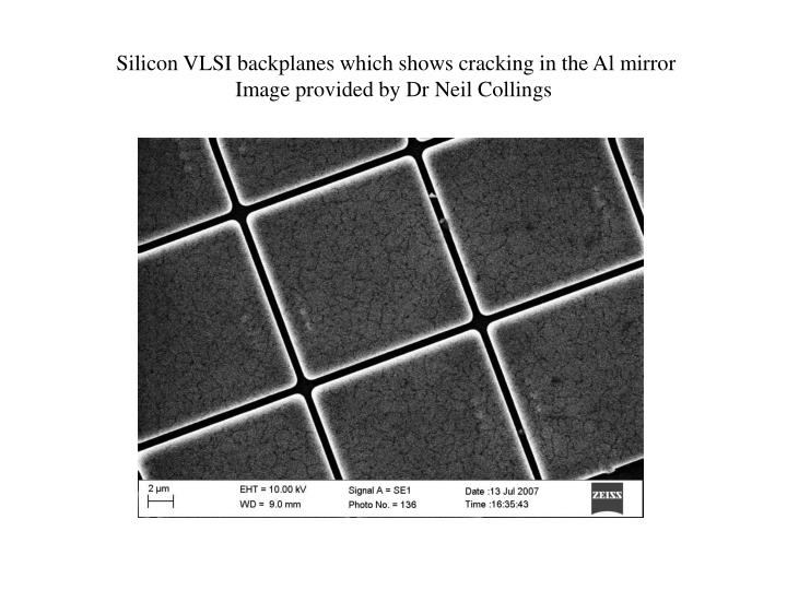
Silicon VLSI backplanes which shows cracking in the Al mirror Image provided by Dr Neil Collings. Silicon VLSI backplanes showing "punch through" of the transistor underlying the mirror. Image provided by Dr Neil Collings.

E N D
Silicon VLSI backplanes which shows cracking in the Al mirrorImage provided by Dr Neil Collings
Silicon VLSI backplanes showing "punch through" of the transistor underlying the mirror. Image provided by Dr Neil Collings
Wafer1.tif: From Mark Mann. First image of CNTs grown by a new type of furnace. This shows morphology and size distribution of the grown nanotubes. SEM was used to compare this across the width of the 4" wafer.
Yps42c1.tif: from Mark Mann. Checking for CNTs grown on the top of sharply etched tungsten contained within a Schottky module. The CNT operates as a field emission source. The SEM is used to check the CNT's length & rough diameter. It also checks for alignment.
Images provided by: Husnu Emrah Unalan Demonstrating supergrowth Further details awaited
Lewis06secondchipTT: Provided by Mark Mann. Fabrication of aligned, sparse arrays of multi-walled carbon nanotubes for use as a field ionizer for mass spectroscopy. Taken at 25 deg. tilt - some tips are >20 um high. They have spacing twice their height for optimum field v current density. The SEM is vital to help achieve a greater uniformity in the grown CNTs.
Vertically aligned Multiwalled Carbon Nanotubes Contributed by Shupei Oei We check by SEM for a) alignment b) growth c) morphology- height, width d) identify tip or base- growth, by observing position of catalyst particle. Resolution is not quite sufficient for for imaging of single walled carbon nanotubes.