Download
1 / 60
600 likes | 759 Views
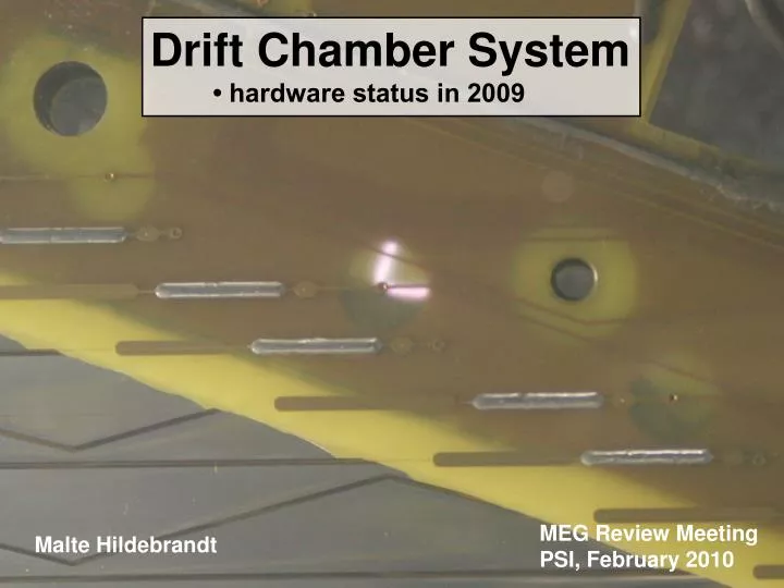
Drift Chamber System • hardware status in 2009. MEG Review Meeting PSI, February 2010. Malte Hildebrandt. Outline. • reminder: HV instability problem in 2007, 2008 • summary of tests and proof of via hypothesis • repair work → new anode pcb → unexpected observations

E N D
Drift Chamber System • hardware status in 2009 MEG Review Meeting PSI, February 2010 Malte Hildebrandt Malte Hildebrandt MEG Review Meeting, 17.02.2010
Outline • reminder: HV instability problem in 2007, 2008 • summary of tests and proof of via hypothesis • repair work → new anode pcb → unexpected observations • installation 2009 • MEG Run 2009 → remaining currents • new cathode foil • Summary / Outlook Malte Hildebrandt MEG Review Meeting, 17.02.2010
Outline • reminder: HV instability problem in 2007, 2008 • summary of tests and proof of via hypothesis • repair work → new anode pcb → unexpected observations • installation 2009 • MEG Run 2009 → remaining currents • new cathode foil • Summary / Outlook Malte Hildebrandt MEG Review Meeting, 17.02.2010
HV Trips Reminder • characteristics of HV trips in 2007 and 2008: • significant deterioration of HV stability started 2007: p at end of run 2008: p beam time (XEC, Dalitz) 2007: after 2-3 months with 2008: after 2-3 months with gas and HV gas and HV → at beginning: same planes affected as in 2007 • further deteriorationduring remaining run time even without any further p beam time 2007: Sep – Dec 2008: May – Dec • stable operation with reduced HV settings 2007: dc system off during 2008: second p beam time p beam time → deterioration due to helium environment ? Malte Hildebrandt MEG Review Meeting, 17.02.2010
HV Tests in 2008 Reminder • tests with dc system in MEG during run 2008: • exchange of infrastructure / hardware (HV module, HV cables) • variation of dp_dc regulation value (pdc-pCOBRA) ↔ small leaks ? • increase ethane fraction in dc counting gas ↔ inside sensitive volume ? • increase air admixture to COBRA ↔ outside dc module ? → no clear cause and effect (on shorterm scale) → but: hint, that problem is connected to longterm exposure to helium Malte Hildebrandt MEG Review Meeting, 17.02.2010
HV Tests in 2009 • tests with dc system in helium cabin • dc system inside helium environment since 16th Jan 2009 • dc modules flushed since 16th Jan: helium since 30th Jan: helium/ethan • operated with MEG dc HV system • goal: investigate HV status • compare with HV status at end of last years run • identify characteristics of weak anode channels • observations (tests finished 11th May): •„weak“ planes (run 2008) got worse •„good“ planes (run 2008) started to deteriorate • all weak anode channels showed same signal characteristics → further proof for assumptions:• HV problem related to exposure to helium • (most likely) same reason for HV instabilities → 4 ½ additional months „run conditions“ after end of run 2008 Malte Hildebrandt MEG Review Meeting, 17.02.2010
HV Tests in 2008/09 Reminder • tests in laboratory (HV test box) • pcb, potting material • helium environment, cHelium > 99% • T ≈ 40-45°C • HV = 2kV • longterm test (>3 months) → no deterioration • finally, only one topic remained on our list of suspicious and possible weak points concerning construction and operation of the drift chambers: → the bottom layer of anode HV pcb where the HV via is facing the GND layer Malte Hildebrandt MEG Review Meeting, 17.02.2010
HV Via top layer GND +HV bottom layer 7 mm Malte Hildebrandt MEG Review Meeting, 17.02.2010
He / C2H6 He air glue glue glue G10 isolator glue G10 isolator glue carbon frame PCB Cross Section bottom layer top layer pcb pcb bottom layer +HV +HV GND Malte Hildebrandt MEG Review Meeting, 17.02.2010
dc01A glue no glue no glue Malte Hildebrandt MEG Review Meeting, 17.02.2010
PCB Cross Section • Why are only certain vias affected? → gas permeability depends on thickness of „barrier“ He / C2H6 pcb pcb +HV +HV GND glue glue G10 isolator glue G10 isolator glue carbon frame Malte Hildebrandt MEG Review Meeting, 17.02.2010
PCB Cross Section • Why are only certain vias affected? → gas permeability depends on thickness of „barrier“ He / C2H6 pcb pcb +HV +HV GND glue glue G10 isolator glue G10 isolator glue carbon frame Malte Hildebrandt MEG Review Meeting, 17.02.2010
PCB Cross Section • Why are only certain vias affected? → gas permeability depends on thickness of „barrier“ He / C2H6 pcb pcb +HV +HV GND glue glue G10 isolator glue G10 isolator glue carbon frame Malte Hildebrandt MEG Review Meeting, 17.02.2010
PCB Cross Section • Why are only certain vias affected? → no breakdown in He/C2H6 (confirmed by test in laboratory) He / C2H6 pcb pcb +HV +HV GND glue glue G10 isolator glue G10 isolator glue carbon frame Malte Hildebrandt MEG Review Meeting, 17.02.2010
dc01 Skeleton in „Aquarium“ • dc01 skeleton: anode middle cathode anode (no hood cathode) • since 19th Feb mounted inside „aquarium“ • 19th Feb – 6th Mar: helium(30 days) 6th Mar – 9th Mar: helium / ethane (3 days) 9th Mar: HV tests („rather“ stable) 9th Mar – 20th Mar: helium (22 days) since 20th Mar: helium / ethane (untill Mar 30th: 10 d) since 23rd Mar: HV tests → 30th Mar: dc01A: first direct / optical observation of discharges between HV via and GND surface on bottom side of HV pcb → characteristics of signals on oscilloscope same as in Jan / Feb when complete dc01 was tested in „aquarium“ but now: no hood, no G10 isolators → 65 days „run conditions“ (up to Mar 30th) Malte Hildebrandt MEG Review Meeting, 17.02.2010
dc01A anode 3 Malte Hildebrandt MEG Review Meeting, 17.02.2010
Outline • reminder: HV instability problem in 2007, 2008 • summary of tests and proof of via hypothesis • repair work → new anode pcb → unexpected observations • installation 2009 • MEG Run 2009 → remaining currents • new cathode foil • Summary / Outlook Malte Hildebrandt MEG Review Meeting, 17.02.2010
HV Print 2009 pads for resistors HV print 2009 • traces for HV on middle layer → no HV traces on bottom layer → individual layers with „only HV“ or „only GND“ (3-layer → 4-layer pcb) • „blind vias“ → vias have only necessary depth to connect appropriate layers (like „blind hole“) print 2007 outer edge inner edge +HV traces vias for +HV GND print 2009 Malte Hildebrandt MEG Review Meeting, 17.02.2010
HV Print 2009 +HV traces in middle layer soldering pads for decoupling capacitors HV print 2009 • soldering pads for capacitors → round shape on inner side where electrodes of capacitor face to each other print 2007 vias for readout connectors print 2009 Malte Hildebrandt MEG Review Meeting, 17.02.2010
HV Print 2009 print 2007 HV print 2009 • tracks and vias for HV on top layer → place HV („blind“) vias close to soldering pads → HV tracks are not covered by small G10 isolator print 2009 print 2007 print 2009 Malte Hildebrandt MEG Review Meeting, 17.02.2010
DC Wing Test Setup • „dc wing test setup“ in HV test box • represents the cross section through wing of dc plane → anode frame – G10 isolators – pcb – G10 isolator – G10 isolator – hood frame • goal: investigate HV stability • discharges due to „polarisation“ effects ? • operated in exhaust line of „aquarium“ → flushed with He/C2H6 • observations: → 14 days with HV thereof: 12 days >2 kV and 7 days 2.6 kV → no HV trips (trip threshold 8mA) Malte Hildebrandt MEG Review Meeting, 17.02.2010
Potting HV Connection → weak point: potting of HV soldering spot on pcb • ThreeBond 1530 (silyl polymer)• EPO-TEK 302-3M (epoxy resin) 2009 2006 - 2008 HV connection to pcb + sealing Malte Hildebrandt MEG Review Meeting, 17.02.2010
DC Repair Work • successful „dc wing test“ was starting signal of dc repair work ↔ all materials were already prepared in advance and on spec • all dc modules were disassembled → middle cathode and cathode hood were recycled without any change → anode frames: • new anode pcb‘s were glued on anode frames • new wires were soldered on the pcbs / frames • assembly of „new“ dc modules → module #1 and #2 operated in „aquarium“ for 6½ months → 16 dc modules for MEG: • each individual chamber tested inside helium cabin with cosmic rays (HV, LV + signal) • complete dc system tested inside helium cabin (only HV) • operation in MEG: 4 months (Sep – Dec) → No deterioration of HV stability during 2009 ! Malte Hildebrandt MEG Review Meeting, 17.02.2010
Outline • reminder: HV instability problem in 2007, 2008 • summary of tests and proof of via hypothesis • repair work → new anode pcb → unexpected observations • installation 2009 • MEG Run 2009 → remaining currents • new cathode foil • Summary / Outlook Malte Hildebrandt MEG Review Meeting, 17.02.2010
Unexpected Phenomena • during disassembly several unexpected phenomena were observed on a limited number of cathode foils and their corresponding anodes: • „damage“ of cathode foil Malte Hildebrandt MEG Review Meeting, 17.02.2010
dc09A Cathode dc09A cathode (foil 42) 1750 V observations: • aluminum coating is peeling off along Vernier pattern • complete length of cell_0 • damaged region: • sharp edges • sligthly extended at etched gaps • not symmetric to anode wire but: „rotation“ of E-field due to B-field in other direction after touching: Malte Hildebrandt MEG Review Meeting, 17.02.2010
dc09A Cathode dc09A cathode (foil 42) 1750 V observations: • aluminum coating is peeling off along Vernier pattern • complete length of cell_0 • damaged region: • sharp edges • sligthly extended at etched gaps • not symmetric to anode wire but: „rotation“ of E-field due to B-field in other direction after touching: → first comment from REPIC: • peeling off maybe due to missing chromium underlayer Malte Hildebrandt MEG Review Meeting, 17.02.2010
dc11B, dc14A – Cathode Foil dc11B hood (foil 22) 1850 V dc14A cathode (foil 25) 1800 V observations: • “spots” / peaks along Vernier pattern • mainly on complete length of cell0, but also at frame edges: cell1, cell2, cell3 and cell4 • damaged region: • sharp edges • sligthly extended at etched gaps • not symmetric to anode wire • anode wires: • mechanical tension ok • → separate transparency • potential wires: ok (?) Malte Hildebrandt MEG Review Meeting, 17.02.2010
dc11B, dc14A – Cathode Foil Al Mg O Al Mg O topography contrast methode scanning electron microscope (SEM) + energy-dispersed x-ray spectroscopy (EDX) S.Ritter (NES/LNM) Malte Hildebrandt MEG Review Meeting, 17.02.2010
dc09, dc11, dc14 dc09A cathode (foil 42) 1750 V dc11A+B cathode (foil 28) dc14A cathode (foil 23) 1800 V observations: • white “shadows” along Vernier pattern • intensity decreasing with r (rate effect?) • not continuous in r, but separated stripes • not symmetric to anode wire • anode wires: • mechanical tension ok • → separate transparency • potential wires: ok (?) 1780 V 1850 V r Malte Hildebrandt MEG Review Meeting, 17.02.2010
dc09, dc11, dc14 dc09A cathode (foil 42) 1750 V dc11A+B cathode (foil 28) dc14A cathode (foil 23) 1800 V observations: • on first sight: like scratches but: • not removable with cotton bud 1780 V 1850 V Malte Hildebrandt MEG Review Meeting, 17.02.2010
dc09, dc11, dc14 dc09A cathode (foil 42) 1750 V dc11A+B cathode (foil 28) dc14A cathode (foil 23) 1800 V observations: • on first sight: like scratches but: tiny „particles“ perfectly aligned along tracks / scratches • not removable with cotton bud 1780 V 1850 V Malte Hildebrandt MEG Review Meeting, 17.02.2010
dc09, dc11, dc14 dc09A cathode (foil 42) 1750 V dc11A+B cathode (foil 28) dc14A cathode (foil 23) 1800 V observations: • on first sight: like scratches but: tiny „particles“ perfectly aligned along tracks / scratches • not removable with cotton bud 1780 V 1850 V scanning electron microscope (SEM) S.Ritter (NES/LNM) Malte Hildebrandt MEG Review Meeting, 17.02.2010
dc09, dc11, dc14 dc09A cathode (foil 42) 1750 V dc11A+B cathode (foil 28) dc14A cathode (foil 23) 1800 V observations: • on first sight: like scratches but: tiny „particles“ perfectly aligned along tracks / scratches • not removable with cotton bud 1780 V 1850 V scanning electron microscope (SEM) S.Ritter (NES/LNM) Malte Hildebrandt MEG Review Meeting, 17.02.2010
dc09, dc11, dc14 foil Al Mg O particle Al (Mg) (O) remark: sample table made of aluminum scanning electron microscope (SEM) + energy-dispersed x-ray spectroscopy (EDX) S.Ritter (NES/LNM) Malte Hildebrandt MEG Review Meeting, 17.02.2010
dc09, dc11, dc14 dc09A cathode (foil 42) 1750 V dc11A+B cathode (foil 28) dc14A cathode (foil 23) 1800 V observations: • on first sight: like scratches → possible reason for scratches: 1780 V 1850 V aluminum polyimide foil Malte Hildebrandt MEG Review Meeting, 17.02.2010
dc09, dc11, dc14 dc09A cathode (foil 42) 1750 V dc11A+B cathode (foil 28) dc14A cathode (foil 23) 1800 V observations: • on first sight: like scratches → possible reason for scratches: 1780 V 1850 V sheet of paper polyimide foil → improve packaging for further delivery: soft, slightly sticking foil instead of sheet of paper Malte Hildebrandt MEG Review Meeting, 17.02.2010
Unexpected Observations • during disassembly several unexpected phenomena were observed on a limited number of cathode foils and their corresponding anodes: • „damage“ of cathode foil • coating on anode wires Malte Hildebrandt MEG Review Meeting, 17.02.2010
dc11B, dc14A – Anode Wires new wire Ni balance Cr 18 - 20% Si 1.5% Al 1000ppm, Fe 2000ppm, Mn 2000ppm Ni EHT = 10 kV Cr (C) Ni Cr Si Ni/Cr (80/20) 25 mm EHT = 20 kV Ni Cr (C) Ni Cr Si remark: C maybe due to sticker on sample table scanning electron microscope (SEM) + energy-dispersed x-ray spectroscopy (EDX) S.Ritter (NES/LNM) Malte Hildebrandt MEG Review Meeting, 17.02.2010
dc11B, dc14A – Anode Wires Ni/Cr (80/20) 25 mm Ni Cr (C) Ni Cr Si O C O Cr Ni Cr Ni Si scanning electron microscope (SEM) + energy-dispersed x-ray spectroscopy (EDX) S.Ritter (NES/LNM) Malte Hildebrandt MEG Review Meeting, 17.02.2010
Unexpected Observations • during disassembly several unexpected phenomena were observed on a limited number of cathode foils and their corresponding anodes: • „damage“ of cathode foil • coating on anode wires • evaluation of the damage: • effects are limited to a very small number of cathode foils / anode wire frames • damage of cathode foil as well as coating on anode wires did not deteriorate the performance of the specific chamber ↔ theses modules were operated at nominal / nearly nominal HV until the end of the run 2008 → check carefully for dc modules which will be disassembled this spring shutdown Malte Hildebrandt MEG Review Meeting, 17.02.2010
DC Repair Work February – April • „dc skeleton“ in aquarium • discussion/design/tests of new anode pcb May – July • construction of new dc‘s → test 2 new dc‘s in aquarium → test of mounted dc modules in support structur July • middle of July: 16 dc modules in support structure → close helium cabin • end of July: repair / construction work finished (2+16) August • further tests, prepare support structure and reserve 1st September → installation of dc system in MEG experiment • summary of dc repair work: 2 dc modules in „aquarium“ for longterm test 16 dc modules in MEG experiment 3 sets of spare frames (modules with damaged cathode foil) → order new foil Malte Hildebrandt MEG Review Meeting, 17.02.2010
Outline • reminder: HV instability problem in 2007, 2008 • summary of tests and proof of via hypothesis • repair work → new anode pcb → unexpected observations • installation 2009 • MEG Run 2009 → remaining currents • new cathode foil • Summary / Outlook Malte Hildebrandt MEG Review Meeting, 17.02.2010
Strain Relief at Inside PatchPanel • location: signal / LV cables inside patch panel • problem: missing dc signal channels / LV channel (2006, 2007) → shutdown 2008: improve strain relief of cables on pcb with aluminum clamps → no LV lost, reduced number of missing signal channels → but: weak point shiftet to the connector/socket on patch panel pcb • installation 2009: 1 signal cable pcb completely disconnected 1 partially disconnected → intensive repair work to fix and to recover ~24 signals (endoscope, sawing, sealing, …) → shutdown 2010: improve strain relief of signal cable pcb on patch panel pcb with bracket Malte Hildebrandt MEG Review Meeting, 17.02.2010
Outline • reminder: HV instability problem in 2007, 2008 • summary of tests and proof of via hypothesis • repair work → new anode pcb → unexpected observations • installation 2009 • MEG Run 2009 → remaining currents • new cathode foil • Summary / Outlook Malte Hildebrandt MEG Review Meeting, 17.02.2010
DC Performance 2009 • dc04B: • cosmic test in laboratory: • nominal HV, normal puls height • during MEG run: • nominal HV, but: low gas gain (I ≈ 0.2·Inormal) • cosmic run in MEG (Jan2010) • nominal HV, normal puls height → not yet understood • dc08B: • cosmic test in laboratory: • nominal HV, no HV trips • at beginning of MEG run: • nominal HV, periodic HV trips: 1 per 1-2d • during MEG run • 3 weeks stable, then again: 1 per 1-2d • cosmic run in MEG (Jan2010) • nominal HV, no HV trips → charging up effect ? • dc04, dc05, dc06, dc11: MEG run: • increasing dark / remaining currents → reduced HV, but still >1800V → replace during spring shutdown • all other dc modules on nominal HV → 30 / 32 planes on HV >1800V! • 4 months operation with flushing gas • 3½ months operation with HV and rate Malte Hildebrandt MEG Review Meeting, 17.02.2010
Dark / Remaining Currents • observations:• some dc planes show dark / remaining currents (up to several mA) • current starts during high rate irradiation • remaining current stays, even when irradiation has finished • only if HV is reduced to 1300V, remaining current dies away remark: no gas gain below ~1300V Malte Hildebrandt MEG Review Meeting, 17.02.2010
Dark / Remaining Currents dc14A Malte Hildebrandt MEG Review Meeting, 17.02.2010
Dark / Remaining Currents • observations:• some dc planes show dark / remaining currents (up to several mA) • current starts during high rate irradiation • remaining current stays, even when irradiation has finished • only if HV is reduced to 1300V, remaining current dies away remark: no gas gain below ~1300V → hint: • self-sustaining discharge (not surface current, …) → certain primary charge density necessary to start gaseous discharge → once started it remains even without source of primary charge • Malter effect:e- multiplication at anode wire (1st Townsend coefficient) e- emission at cathode due to field emission Malte Hildebrandt MEG Review Meeting, 17.02.2010
Malter Effect cathode cathode anode wire 1 2 anode wire + e-→ e-→ ← + + + + + + + isolating film / layer isolating film / layer • insulating film / layer on cathode • primary charge due to irradiation • motion of charge due to electrical field • small surface conductivity → rate of charge build up higher than its removal rate Louis Malter, Phys.Rev. 50 (1936) 48-58: Thin Film Field Emission Malte Hildebrandt MEG Review Meeting, 17.02.2010