Download
1 / 19
230 likes | 541 Views
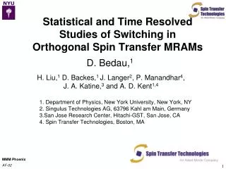
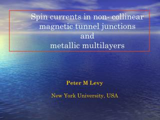
Ultrafast Switching in Magnetic Tunnel Junction based Orthogonal Spin Transfer Devices. H. Liu [1]* , D. Bedau [1] , D. Backes [1] , J. A. Katine [2] , J. Langer [3] , and A. D. Kent [1] [1] Department of Physics, New York University, New York, NY 10003 USA

E N D
Ultrafast Switching in Magnetic Tunnel Junction based Orthogonal Spin Transfer Devices H. Liu[1]*, D. Bedau[1], D. Backes[1], J. A. Katine[2], J. Langer[3], and A. D. Kent[1] [1] Department of Physics, New York University, New York, NY 10003 USA [2] San Jose Research Center, Hitachi-GST, San Jose, California 95135 USA [3] Singulus Technologies AG, 63796 Kahl am Main, Germany *: presenter Appl. Phys. Lett. 97, 242510 (2010) March Meeting 2011, Dallas TX
Outline • Sample • Design • Goal: fast, reliable switching • Why orthogonal geometry? • Sample • Characteristic • Sample structure • Coercive field and energy barrier • Switching • Measurement • Fast, reliable switching • Unique behavior March Meeting 2011, Dallas TX
Switching in collinear devices • Initially: • No spin torque, if no thermal fluctuation • Waiting for large thermal fluctuation • Incubation delay (~ns) • Unpredictable switching process • During the switching process: • In – plane: complicated trajectory • Perpendicular: fastest motion(precession) doesn’t contribute to switching m mp Polarizing layer electron Switchable layer March Meeting 2011, Dallas TX
Switching in orthogonal devices A.D. Kent et al., Appl. Phys. Lett. 84, 3897(2004) -Bdemag t=T/2 t=T • Merits: • Large initial torque. • Fast switching process. • Deterministic switching. • Low power consumption. t=0 Current • Differences from collinear: • Bipolar switching. • Non – monotonic switching probability distributions March Meeting 2011, Dallas TX
Sample structure Appl. Phys. Lett. 97, 242510 (2010) SAF: PtMn CoFe Ru (AF coupled) CoFeB Barrier: MgO Free layer: CoFeB (3 nm) Spacer: Cu Polarizer: CoNi/CoPd Size: 40 nm x 80 nm ~ 80 nm x 240 nm. Shape: rectangles, ellipses and hexagons. Measured: hundreds of samples. Present: a typical 60nm x 180 nm hexagon March Meeting 2011, Dallas TX
Hysteresis March Meeting 2011, Dallas TX
Estimate energy barrier fit March Meeting 2011, Dallas TX
Magnetic field Fast switching measurements Switching only happen during the current pulse 1 2 Current Pulse Measure R Measure R’ 3 Compare R, R’ not switch 2 switched 3 2 1 Apply the same pulse 100 – 10,000 times March Meeting 2011, Dallas TX
Fast switching • Fast switching • 100 % under 500 ps • No nano-seconds incubation delay • Low energy cost • -0.6 V, 500 ps • 400 Ω < R < 800 Ω • 225 fJ < E < 450 fJ Appl. Phys. Lett. 97, 242510 (2010) March Meeting 2011, Dallas TX
Bipolar and non–monotonic • Bipolar switching: • Appears for both P-> AP and AP-> P switching • The torque originates from the perpendicular polarizer • Heating is not an importantmechanism since SP is different for different polarities • Non – monotonic switching: • Clearly appears in P -> AP switching with Vp > 0 and AP -> P switching with Vp< 0 • Qualitatively consistent with the deterministic switching Appl. Phys. Lett. 97, 242510 (2010) March Meeting 2011, Dallas TX
Switching in zero effective field • Another sample • Size: 50 nm x 100 nm • Shape: rectangular • Also fast • ~100% at 1 ns • Also Low E • 0.75 V, 1 ns • 2.2kΩ < R < 4.5kΩ • 125 fJ < E < 256 fJ March Meeting 2011, Dallas TX
Conclusion • We have fabricated OST-MRAM devices that incorporate a magnetic tunnel junction. • 100% switching probability is reached for pulses shorter than 500 ps requiring an energy < 450 fJ. • Due to the perpendicular polarizer switching is possible for both pulse polarities. • Precessional switching has been observed in the non-monotonic behavior of the switching probability versus pulse amplitude. Appl. Phys. Lett. 97, 242510 (2010) March Meeting 2011, Dallas TX
Thank you ! March Meeting 2011, Dallas TX
Switching in zero effective field 50 nm x 150 nm rectangular Hc = 8.5 mT A = -0.45 V March Meeting 2011, Dallas TX
Material hysteresis March Meeting 2011, Dallas TX
Magnetic field Fast switching measurements Switching only happen during the current pulse 1 2 Current Pulse Measure R Measure R’ 3 Compare R, R’ not switch 2 switched 3 2 1 Apply the same pulse 100 – 10,000 times March Meeting 2011, Dallas TX
Spin Torque • Spin torque – the amount of transverse angular momentum transferred in unit time. e mp electron m magnetization March Meeting 2011, Dallas TX
Spin Transfer Devices Memory 1 Memory 2 Oscillator / Memory Kent et al., APL (2004) Ebelset al., Nat. Mat (2007) Lee et al., APL (2009) Papusoi et al., APL(2009) Beaujour et al., SPIE(2009) Mangin et al., Nat. Mat. (2006) Mangin et al., APL (2009) Sun, PRB (2000) Bedau et al., APL (2010) March Meeting 2011, Dallas TX