Download
1 / 10
100 likes | 284 Views
Chapter 14-1. Metal-semiconductor (MS) junctions. Many of the properties of pn junctions can be realized by forming an appropriate metal-semiconductor rectifying contact (Schottky contact) Simple to fabricate Switching speed is much higher than that of p-n junction diodes

E N D
Chapter 14-1. Metal-semiconductor (MS) junctions • Many of the properties of pn junctions can be realized by forming an appropriate metal-semiconductor rectifying contact (Schottky contact) • Simple to fabricate • Switching speed is much higher than that of p-n junction diodes • Metal-Semiconductor junctions are also used as ohmic-contact to carry current into and out of the semiconductor device
Ideal MS contacts • Assumptions - Ideal MS contacts • M and S are in intimate contact, on atomic scale • No oxides or charges at the interface • No intermixing at the interface
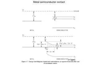
MS contacts • Vacuum level, E0 - corresponds to energy of free electrons. • The difference between vacuum level and Fermi-level is called workfunction, of materials. • Workfunction, M is an invariant property of metal. It is the minimum energy required to free up electrons from metal. (3.66 eV for Mg, 5.15eV for Ni etc.) • The semiconductor workfunction, s, depends on the doping. • where = (E0 – EC)|SURFACE is a a fundamental property of the semiconductor. (Example: = 4.0 eV, 4.03 eV and 4.07 eV for Ge, Si and GaAs respectively)
Energy band diagrams for ideal MS contacts (a) and (c) An instant after contact formation (b) and (d) under equilibrium conditions M > S M < S
MS (n-type) contact with M > S • Soon after the contact formation, electrons will begin to flow from S to M near junction. • Creates surface depletion layer, and hence a built-in electric field (similar to p+-n junction). • Under equilibrium, net flow of carriers will be zero, and Fermi-level will be constant. • A barrier B forms for electron flow from M to S. • B = M – ... ideal MS (n-type) contact. B is called “barrier height”. • Electrons in semiconductor will encounter an energy barrier equal to M – S while flowing from S to M.
MS (n-type) contact with M > S Response to applied bias for n-type semiconductor Note: An applied positive voltage lowers the band since energy bands are drawn with respect to electron energy.
I VA MS (n-type) contact with M < S • No barrier for electron flow from S to M. So, even a small VA > 0 results in large current. • As drawn, small barrier exists for electron flow from M to S, but vanishes when VA< 0 is applied to the metal. Large current flows when VA< 0. • The MS(n-type) contact when M < S behaves like an ohmic contact.
Example Find barrier height, built-in voltage, maximum E-field, and the depletion layer width at equilibrium for W-Si (n-type) contact. Given: M = 4.55eV for W; (Si) = 4.01eV; Si doping = 1016 cm3 Draw the band diagram at equilibrium. Solution: Find EF – EiEF – Ei = 0.357eV Find EC – EF EC – EF = 0.193eV B = M – = 0.54eV Vbi = 0.347 V W = 0.21 m E(x = 0) = Emax = 3.4 104 V/cm